Introduction: Build a Computer W/ Basic Understanding of Electronics


Have you ever wanted to pretend you were really smart and build your own computer from scratch? Do you know nothing about what it takes to make a bare-minimum computer? Well, it is easy if you know enough about electronics to throw some ICs together correctly. This instructable will assume you are good at that part, plus a few other things. And if not, it still shouldn't be too difficult to follow along if you know how breadboarding/prototyping is done. The purpose of this instructible is to get you a working "computer" without knowing a whole lot about how they work. I will cover wiring and basics of programming, as well as provide a very short program for you. So let's get started.
Step 1: Parts and Stuff


A "computer" requires: power, input, processing, memory and output. Technically we will have all of these things. I shall cover these things in that order.
For power, you will need a 5 volt (hereon labeled as 5V) source. It is recommended it be a regulated source so you don't accidentally fry parts in your circuit. Our input will be buttons. Processing is self-explanatory; we're using a processor. Memory will only consist of ROM. The processor's internal general purpose registers will be enough to use as RAM. Output will be LEDs.
1 LM7805C - 5V Regulator
1 ZYLOG Z80 - Processor
1 AT28C64B - EEPROM
1 74LS273 - Octal D Flip-Flop
1 74HC374E - Octal D Flip-Flop
3 CD4001BE - Quad NOR Gate
1 NE555 - Clock Generator
2 1K Ohm Resistor
1 10K Ohm Resistor
1 10K Ohm Resistor Network; 8 Bussed OR 8 Additional 10K resistors
1 1uF Capacitor
1 100uF Capacitor
1 Push Button
1 3x4 Button Matrix OR 8 Additional Push Buttons
8 LED - Color Choice Doesn't Matter
8 330 Ohm Resistors or Resistor Network
1 Really Big Breadboard or Multiple Small Ones
Lots and Lots of Wire
In my schematic I have a stick of SRAM installed. You do not need to even worry about that. I only added it to the schematic to accurately reflect my actual circuit and I added it to the circuit for future use. Also added to the schematic is a quad OR gate (74LS36). The two unused gates' inputs are tied to VCC and their outputs left floating (not drawn). Also not drawn nor listed above are two capacitors on the power circuit.
I am feeding regulated 12V into the 5V regulator to feed the entire breadboard. It gets rather warm, so I attached a heat sink to cool it. If you use less than 12V to feed the regulator (use at least 7V), it should run cooler.
The Z80 is where the magic happens. It takes instructions stored in ROM and executes them. The EEPROM stores our program for the processor to execute.
The octal flip-flop that is our output device that latches the data on the data bus to its own output. This allows us to change whats on the bus, which is a very important step done multiple times per instruction, without changing what the user/viewer sees. The flip-flop can not drive the current required to light the output LEDs, so they feed into two of the quad NOR gate chips which act to buffer the 8 data lines to drive the LEDs. Since they output of the gates are inverted, we also have to wire the LEDs to be inverted, but we'll come to that when we come to that. The other NOR chip is used for logic decoding but only three gates are used.
The octal flip-flop used for input is essentially the same thing. The output flip-flops hold their output either high or low so it can't be used to drive the bus; it would hold data on the bus. The flip-flop used for input replaces the /RESET pin with /EN, which more or less disconnects the outputs of (and from) the chip so it won't hold data (tri-state outputs).
Step 2: Wiring the Power, Clock and Reset Circuits


NOTE: For all parts, wire the power rails first. Of all things to forget to wire, the chips will be much less likely to survive forgotten power connections.
The power circuit is the most simple circuit to wire, followed by the reset and clock circuits, respectively. In the picture, the 12V input is on the power strip to the far right. The brown wire, hiding a yellow one underneath it, feeds the 12V to the regulator. The output of the regulator feeds every other power strip on the breadboard and every power strip share a common ground because that's how electronics work.
The processor requires a clock circuit to operate. Without it, it will just sit there in its initialized state and do nothing. The clock operates the processors internal shift registers so it can generate the signals to do stuff. Any clock input will do, even a simple resistor and push button. But it takes many clock cycles to execute instructions. The instruction to write to the output takes 12 cycles in itself. You probably don't want to sit there and press a button 100+ times to get just one loop of the code (actual numbers are at the end of the instructable). That's what the NE555 is for. It does the switching for you and it does so at a (relatively) fast rate.
Before you start wiring anything, you may want to go ahead and figure out how you want your components layed out on the board. My clock circuit is kinda just put at the bottom of the board so it would be out of the way of other components. We will assume you know how to make a basic clock with the timer. If you do not, you will want to look up "555 Astable" and follow a tutorial. Use the 1K resistor to go between the 5V rail and pin 7 of the timer (R1) and the 10K between pin 7 and pin 2 (R2). Make sure to tie the reset pin, pin 4, to the 5V rail so the timer can function. I put an LED on the output of mine so I could verify that the clock did in fact work, but it isn't needed.
Another option with the NE555 is to set it up as a NOT gate and use a 1K resistor to tie the output back to the input. It is usually recommended to use 3 timers to do this, but I found that just 1 should work fine. Just know that if you do this, it will oscillate at a very high speed and it will be very difficult, impossible even, to tell that the output LEDs are flashing. This setup is called a "ring oscillator."
Do note that we are not connecting the clock to the processor yet. We are simply getting it ready. Also note the logic chip just above the clock in the image. It was added way later and that was the only semi-reasonable spot left to place it. It is used for RAM/ROM selection. This instructable ignores RAM so you will not have this chip on your board.
Now we wire the reset circuit. First you need to find a spot on your board for it. I chose right beside the clock. Add your button to the board. Use a 1K resistor to tie one side of the button to the 5V rail. Our RESET pins are active low, meaning we need to hold them high. That's what the resistor is for. This junction is also where the reset pins connect. The other side of the button goes straight to ground. If you want power-on reset, add the 10uF capacitor to this junction too. It will keep the voltage on the reset pins low long enough to activate the reset circuitry within the processor and flip-flop.
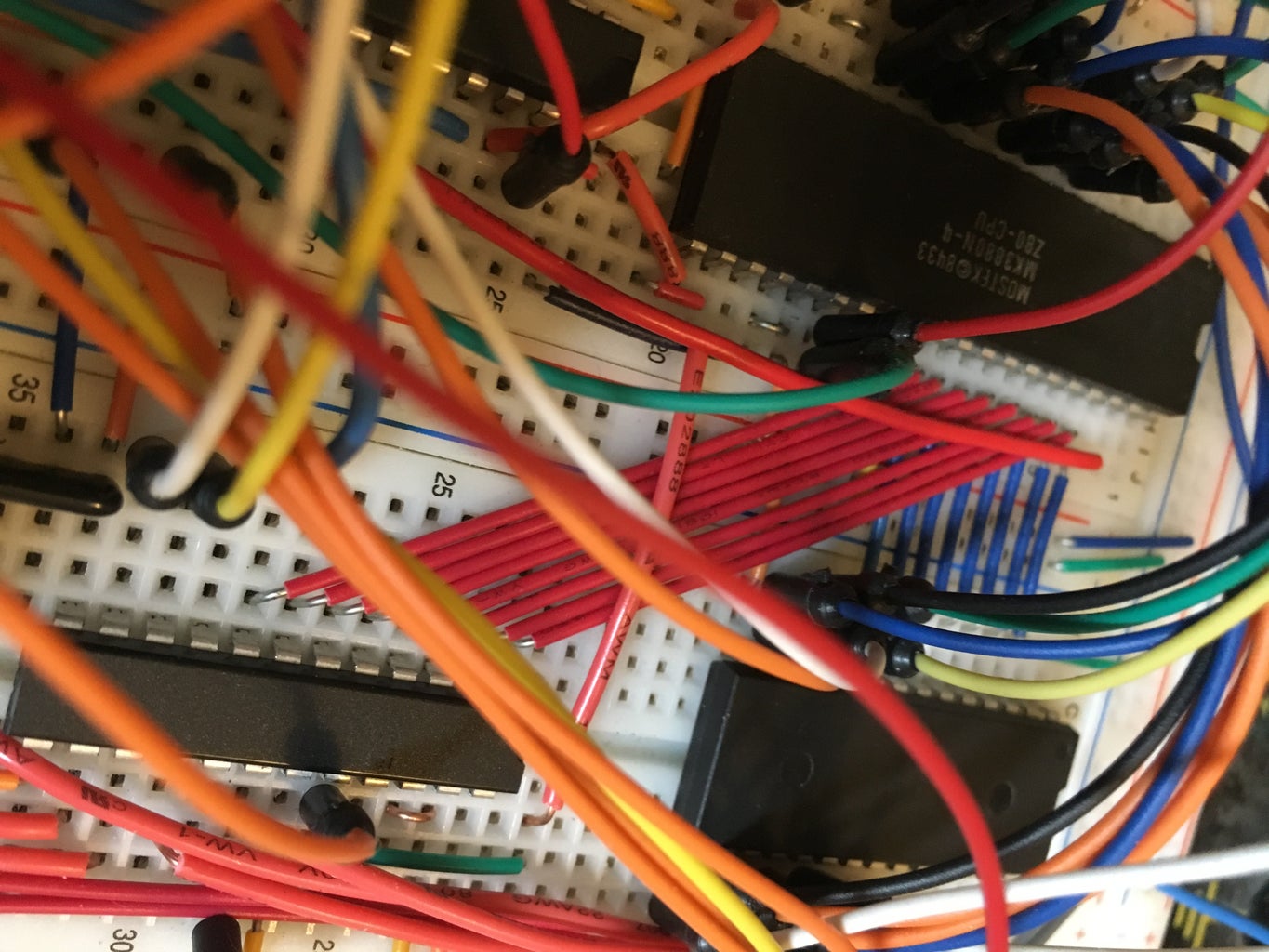
Step 3: Wiring the Z80
Now we get to the nitty-gritty. We shall wire the beast that is the Z80. On my board, I put the Z80 at the top on the same section of board as the reset circuit. As stated previously, wire the power rails first. 5V goes to pin 11 on the left and ground is one pin down but on the right. You may have also noticed the odd width of the chip. It will cause you to have 3 open connectors on one side on the breadboard and 2 on the other. It only makes it less convenient to wire additional stuff if you choose to do so.
The following pin numbers--I assume you know how to count pins on an IC--are unused inputs and must be tied to the 5V rail: 16, 17, 24, 25.
Remember our clock? Its ouput goes to pin 6 on the z80. The reset circuit connects to pin 26. Without having the other components on the board, this is as far as I can get you with the wiring of the z80 itself. More wiring done to it will be done in later steps.
Because I had already had the circuit built before I even considered writing this instructable, I will hold off on the picture until the next step.
Step 4: Wiring the ROM
NOTE: You may want to hold off on actually placing it on the board if it still needs programmed (more on that later).
For the ROM, I placed it beside the Z80 on the right and also displaced it one pin down on the breadboard. This allowed me to wire the address bus directly over, but more on that later. The AT28C64B is an EEPROM, meaning it can be programmed multiple times by switching some pins off and on. We don't want our EEPROM to accidentally reprogram itself when it's in the circuit. So once you have your power rails hooked up, wire pin 27 (/WE) to the 5V rail to disable the write feature altogether.
My program is so small, I only needed the lower 5 address lines (A0-A4) connected, but I wired A5, A6 and A7 anyway so I can write bigger programs without additional work. The additional address lines (A8-A12) are tied directly to ground to prevent unwanted access to the higher addresses from floating inputs. With the unused address inputs tied to ground and the write control tied to 5V, wiring the rest is rather straightforward. Find A0 on the processor and wire it to A0 on the ROM. Then find A1 on the processor and wire it to A1 on the ROM. Do this until you wired all the addresses together. In the image, my address bus to the ROM is done in blue wiring. The address bus going to the RAM is done in red wiring. These wires were all pre cut and stripped as they came in a breadboard wiring kit and were perfect for this wiring.
After you get the addresses wired (this is called the address bus), do the exact same thing for the pins labelled D0, then D1, D2, etc. Do this for all of the data pins (D0 - D7) and you have your data bus wired. We are almost done wiring the ROM. Find the ROM's /CE (chip enable) pin and wire it to the processors pin 19, /MREQ (memory request) and then find the ROM's /OE (output enable) and wire it to processor pin 21, /RD (read). We are now done. All of these are done with jumper wires because they have to go to the other side of the processor and a breadboard does not offer enough room to use neat wiring like that.
Step 5: Wiring the Output


Because it was unpopulated, I chose the section of board to the left of the Z80 for the output. Place the flip-flop on there and connect them power rails. Pin 1, /MR (reset) can connect directly to the reset pin of the processor, but you can leave it tied to the 5V rail. Doing this will only cause it to show junk data until the first write. Notice how the chip has a clock input on pin 11. This input is weird in that it is activated when the pin goes high. Also note that this pin is NOT the same clock that drives the processor. This clock latches the data asserted on the data bus.
Remember how we connected D0 - D7 on the ROM to the same pins on the processor? Do the exact same for this chip. Its D0 goes to D0 on the data bus and so on. The pins that begin with a "Q" are outputs. Before we wire those, we need to add more chips. I used the quad NOR gates because I have a tube of them and I already needed one, but about any chip will work if you wire it correctly. I could have tied one input on all gates to ground and used the other inputs as, well, inputs, but I chose to wire both inputs together for simplicity.
I placed the chips below the flip-flop to make it easier to wire directly without jumpers but I was running low on wire at this point so it didn't really matter in the end. The Q0, Q1.....Q7 on the flip-flop goes to the inputs on the individual gates. With 4 gates in each package/chip, I needed 2 packages and used all gates. If you find a version of the flip-flop that can drive the LEDs without needing buffered like this, these two chips are not needed. If you use gates as a buffer that do not have inverted outputs (AND/OR/XOR), then you can wire the LEDs as you would expect. If you're using the same parts as me and/or the outputs are inverted, the LEDs should be wired as described below. The first image shows the IC portion of the output.
Use the 330 Ohm resistors to tie the LEDs positive (Anode) to the 5V rail and connect the negative (cathode) to the output of the gates. You can see in the second image that I used two resistor buses, each with only five internal resistors. Wiring the LEDs like this will make them light up when the output is off. We do this because the output is off when the input is on. Make absolutely sure that you keep track of which gates your outputs from the flip-flop control. Unless your LEDs will be scattered or their order is meaningless, losing track of them can cause confusion later on when you're asking yourself why the output is wrong.
Step 6: Wiring the Input

Take that 74HC374 flip-flop and place it somewhere. Mine was somewhere below the Z80 towards the bottom of the board. Remember last time when we connected D0 to D0 and D1 to D1 and so on? This time we connect Q0 to D0 and Q1 to D1 and so on. Thankfully we don't have to add any buffer chips this time, haha. Instead we are going to connect a 10K Ohm to each "D" pin (D0-D7) and ground and then a button to the same pins and the 5V rail. Or you can use a resistor bus and reduce your part count a lot. A 3x4 button matrix (without a matrixed output!!) will help too. The image shows the entirety of the input circuit along with the glue logic (that part is next).
Step 7: Glue Logic
We have one last thing to wire. It's called "glue logic" because it is used to decode control signals to make it all work; it's what holds the circuit together. When the processor wants to write data to the output, both /IORQ and /WR (20 and 22 respectively) go low and the data being sent is asserted on the data bus. The clock pin on both flip-flops are active high, meaning the data is latched when the pin receives a high signal. We use a NOR gate and wire /IORQ to one input of the gate and /WR to the other input. When either is high, meaning the IO circuits aren't being selected or a write operation isnt being performed, the output feeding the clock of the flip-flop remains low. When both inputs are low, and only when, the output goes high and the flip-flop latches the data.
Now we need to wire the input flip-flop. We can wire the clock pin in much the same way as the previous, but using /IORQ and /RD. But unlike the other flip-flop, we also have a /OE pin that needs taken low only when /IORQ and /RD are low. We could use an OR gate. Or we could just take the signal we already have for the clock and invert it with one of the two inverting gates we already have available. At the time of stating this instructable, I did not have an OR gate available, so I used one the latter option. Using the latter option meant I didn't need to add any additional parts anyway.
Step 8: Programming
Should your wiring be correct and my explanation clear, all that's left is to get the ROM programmed. There are a few ways to go about this. You could take the easy way and order a new chip off of Digikey. When you're ordering the part, you will have the option to upload a HEX file and they'll program it before they ship it. Use the HEX or OBJ files attached to this instructable and just wait for it to arrive in the mail. Option 2 is to build a programmer with an Arduino or something. I tried that rout and it failed to copy certain data correctly and it took me weeks to figure that out. I ended up doing option 3, which is to program it by hand and flip switches to control the address and data lines.
Once converted directly to the OP Code of the processor, this entire program rests in only 17 bytes of address space, so programming by hand wasn't too awful. The program loads into general purpose register B the value of 00. Register B is used for storing a result of the previous add. As the A register is where math happens, we will not use it to store data.
Speaking of the A register, we perform an IN command, which reads the input, and store the read data in A. Then we add the contents of register B and output the result.
After that, register A is copied into register B. And then we do a series of jump commands. Because all the jumps point to the lower byte of the address lines, and because the upper byte of the jump instruction is given in the second argument and is "00," we can force each jump to be followed by a NOP. We do this to give time between showing output and reading input to prevent accidental input. Each jump uses ten clock cycles and each NOP uses four. If the loop takes too long for your liking, you can increase the clock speed or you can reprogram it to use one less jump.
Attachments

Step 9: Testing
If you wired everything correctly and your ROM is programmed correctly, there is one final step to take: plug it up and see if it works. Press a button and wait a few seconds. It takes 81 clock cycles for the program to reach its first loop and each loop takes 74 clock cycles.
If it doesn't work, check for shorts and unconnected pins (opens) and other wiring issues. If you opted out of power-on reset, you will need to do a manual reset before the processor does anything. You can also attach LEDs to the address bus to see if they're behaving. I was having issues with that myself, so I stuck them directly to the data bus instead. This allowed me to see what was being communicated between the processor and ROM without needing to worry about if the ROM was being read correctly, which would have required timing diagrams and I just didn't want to get that involved. Turns out to have been a good choice because I finally caught the problematic OP Codes that were stored incorrectly.