Introduction: NFC Lock - When a PCB Is Also the Buttons, the Antenna and More...
You can take one of two things from this Instructable. You could follow along and create your own combination of a numeric keypad and a NFC reader. The schematic is here. The PCB layout is here. You'll find a bill of materials for you to order the parts you need. I've provided the code for programming the microcontroller. There's everything you'd need to copy or extend this project.
However, I suspect most readers are more likely to just take inspiration from some aspects of it. This Instructable shows you that the PCB is more than just a way to wire the components together. That little rectangle of fibreglass and copper has plenty of other uses - whilst still taking on its main job of making electrical connections. I'll present all these aspects first before pulling them together into a completed project. I hope you enjoy the journey and may decide to use one or two of these tricks in a project of your own!
Step 1: The Process
So many projects take the same trajectory on the path to "finished" and so many stumble right before the final hurdle.
The prototype
First there's the prototype. You have an idea and out of the drawer comes your go-to microcontroller development board. For many this will be an Arduino, but I'm happiest around TI's MSP430 line of 16-bit low power microcontrollers. Whatever your choice, there's usually a development board that helps. It means you don't have to start with making your own PCB and you can test out theories and potential peripherals. There's often a Booster Pack / Shield / Hat - or whatever strange name for a daughter board the manufacturer has come up with. None of use are strangers to a breadboard or stray wire.
You can see that here I've used TI's CapTIvate development kit and TRF7970A NFC Booster pack to prove that the concept is likely to work.
You'll knock up some proof of concept code too. It may be messy. It may rely on downloaded libraries that get you part of the way there. Personally, I tend to leave it a little imperfect because I know I have those weeks ahead waiting for the PCBs to arrive. I can tidy it up then.
The design
Next comes the design. Fire up your favourite PCB design software. In my case it's Eagle. It takes a surprising amount of time to go from idea to perfection, and here's where our adventure lies! The coming steps will help you get the most out of this.
Waiting for your PCBs
You might etch your own or get them made in a hurry, but most of us will order from a board house in China and wait a few weeks. Now's the time to get back to that code. It won't tidy itself!
Assembly and debugging
Get the soldering iron or toaster oven out. Then you can see if it works as expected. Maybe go back 2 steps. Maybe not.
The enclosure and front panel
So your PCB looks professional. Now it need an enclosure and front panel. Maybe you'll 3D print something. It looks OK-ish, but it doesn't quite represent the finesse of the lovely PCB inside. Well, here's where this guide is really going to help!
Step 2: Your PCB As the Front Panel
Soldermask used to just be green. Silk screen was functional rather than decorative. A PCB was something that was hidden away and only geeks like us would be interested in seeing it. Well, not any more!
Many board houses now allow you to pick from a wide range of colours. Silk screen quality has improved a great deal. Funky shapes and cutouts are allowed. So why not take advantage of this? If you create the PCB carefully then a board house can make your front panels for you!
In my example, I have placed all the components on one side and made sure the other side looked good enough to be the front of my device. You don't have to do this. Maybe you want to have the beauty and the brains on separate boards. It's up to you.
I've even seen a number of PCBs soldered together to form the whole enclosure, but that's unusual. If you think you can do it though - why not!
My board is fairly simple - just some neat white silkscreen over a black soldermask. It suited the look I was after. It is possible to get quite a range of colours and shades by combining silkscreen, soldermask and copper in various ways. I'll leave you to Google "PCB art" and see some of the amazing creations other people have come up with! Impressive though they are, maybe not all are suitable for a front panel.
Step 3: Your PCB As the Buttons
You may have noticed that the silkscreened numbers look a lot like a numeric keypad and that's because they are. To be precise they're capacitive touch buttons. If you're going this route then you will probably want a microcontroller that supports capacitive touch although it is possible to "roll your own" capacitive touch sensing if you really want.
All capacitive touch buttons consist of are some PCB traces that are placed to have a detectable capacitance either to ground (known as self-capacitance) or to another trace (known as mutual capacitance).
I started my design by following TI's CapTIvate guide for their MSP430FR2633 device but if you're using another microcontroller it is probably worth looking at the guides and reference designs provided by the manufacturer. Not only is a guide to the PCB layout provided, but there is even the CapTIvate Design Center that will generate some template code to match your hardware.
You'll notice that the essence of the button is just two circles of copper fairly near each other. Bringing your finger near reduces the capacitance between them. The MSP430 uses a constant current source to charge this capacitor and measures how quickly the voltage across it changes. The CapTIvate library simplifies turning this into detected button presses.
I designed a custom part in Eagle to simplify adding twelve of these buttons and so that I could use them on future projects.
Step 4: Your PCB As an LED Diffuser
The eagle-eyed amongst you may have noticed the small circular patch where the black soldermask is missing from both sides of the PCB. As with almost any electronic design, I needed some visual feedback for the user. I went with an RGB LED and had a few options for this.
- I could use a through-hole LED and cut a hole for it to poke through. I'm not sure how I'd connect it without another PCB.
- I could use a surface mount LED. Then I'd have some traces and an LED messing up my neat front panel.
- I could use a reverse-mount LED.
Some of you may be wondering what a reverse mount LED is. Well it's an "upside down" surface mount LED that shines back at the PCB it's mounted on. What?! Why would you do that? Well, it gets it out of the way on the other side of the PCB. Most designs will still have a hole in the PCB for this LED to shine through, but I decided just to remove the copper and soldermask and see if the PCB material was translucent enough for the LED to shine through. Spoiler alert - it was! I'm sure it would be a bit brighter with a hole instead, but it is easily enough to be visible in sunlight through 1.6mm of FR4. It's nicely diffused too.
It did need a custom part designed it Eagle to ensure that there was no copper or soldermask below it, but all this took was a couple of circles on the Restrict and Keepout layers on both sides. You'll find this custom part in the attached Eagle library.
Step 5: Your PCB As an Antenna
Using a PCB trace as an antenna is nothing new. The NFC Booster pack I used has one. Most commercial NFC readers you'll find use them. One issue I found is that these are tuned to suit the most common NFC tag formats - cards and keyfobs. I'm geeky enough to have a small NFC tag implanted in my hand. Details are here if you're not squeamish. I've also made a previous project using a wire wound inductor as an antenna. For this project I wanted to see if it was possible to create a PCB antenna that was nicely matched to a tiny implanted tag.
Firstly I decided to create a PCB trace that physically smaller than those you'll normally see. The inductance is important when tuning the antenna so I use an online PCB inductor calculator and aimed for about 1μH to be about the same as the wire wound one I'd used before. I used TI's L_Calculate and this told me that 7 turns at an average size of 9mm x 6.5mm with a trace width of 0.1524 should be 950nH. Close enough.
When I got the PCBs back it measured 0.627μH - with a resistance of 0.867Ω. It's time to work out what the matching network should look like so that the TRF7970A sees 50Ω. Antenna matching is a whole topic on its own, so I won't digress into that now, but if you are interested I covered how to tune an antenna without needing an expensive VNA here.
Suffice it to say that your PCB can be used to create a zero-cost antenna whether it's an inductive coil for RFID (not strictly an antenna) or for WiFi, ZigBee, Sub-1Ghz, etc. Once again, I'd suggest that if you need one you start from design notes for whatever device you're using. The manufacturer wants you to buy their components so they are a great help when it comes to making use of them.
Step 6: Your PCB As a Debug Header
As soon as you add a microcontroller to your project you have the issue of how to get your code onto it. Frequently you nice low profile PCB ends up with a chunky pin header on it. Frequently these are through hole versions too, so you lovely neat PCB has been affected on both sides. Obviously as I wanted one side to be my front panel, through hole as out. Surface mount pin headers can risk peeling up your traces - especially if you are likely to connect and disconnect a few times.
Luckily there is an alternative - pogo pins. These spring loaded pins make a nice electrical contact with your board. It might not be quiet enough for a permanent connection but it certainly is for programming. I've seen pogo pins used with a custom jig for both programming and also for testing a production board. I've even seen them stuck on a clothes peg for a very home-made programmer look. However, I made use of a commercial product that's available for many microcontroller families - Tag Connect. It does require a few tiny alignment holes in your board so it might not be perfect if you need a waterproof front panel but I decided that it would be fine for this project.
All that's required is a PCB footprint and you're done! The holes are well within the requirement of a board house and maybe even home etching.
Step 7: The Finished PCB
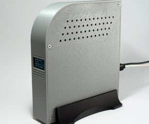
So, after incorporating all of these PCB ideas into one project - here's the final result. It responds to either the correct NFC tag or entry code and opens the door. The door operation is separate because this will operate a couple of different doors in a couple of different ways. The door to my house will be an electromagnetic release, much as you would find on an apartment block with an intercom system.
I'm a kitesurfer so often find myself in the ocean and it's always tricky to know what to do with your keys. With an NFC tag in my hand I always have the key with me! For my van it will link up to the central locking system.
For you own door you may well want to chose an appropriate way to open or unlock it.
You will find everything you need to replicate (or adapt) this project in this GitHub repository.
https://github.com/FredMurphy/LockNFC
I hope you've enjoyed reading about this project and that it has inspired you to incorporate some of the ideas into you own PCBs. If you do, please let me know in the comments below. Please also take a look at the entries in the PCB contest and vote for whichever you think is best. I hope it'll be mine, but I'm sure there are lots of other good entries there too.

Runner Up in the
PCB Contest


