Introduction: 5V Stabilised Supply for USB Hub


This is a stabilised supply intended to be used with a bus powered USB hub in order to deliver a stabilised + 5 volt supply to the devices connected to it.
Due to the resistance of the connecting cable, and the resistances introduced for current sensing for overcurrent protection, the voltage at the hub can be anywhere between +4.5 V(loaded) and +5.5 V. This circuit will deliver a stabilized +5 V in both the cases, ie, it is a buck/boost design, using the TPS63000 switch mode regulator chip manufactured by Texas Instruments.
It can deliver +5 V at 500 mA from input voltages as low as 2 Volts so a rechargeable battery and its (USB powered) charger can be added to make this into a USB UPS for the USB hub.
Step 1: Preparing the Circuit Board

I decided to do a ground plane based layout. The chip has ten solder pads and a thermal pad to be soldered, and this was a different method to try with these types of leadless packages.
A scrap of single sided paper phenolic copper clad was cut to size and the outline of the chip drawn on its unclad side.
Then with a small screwdriver sharpened into a chisel, material was removed, making a niche for the chip to sit in.
Step 2: Gluing the Chip In

The chip is then glued into the space so dug out.
This is, strictly speaking, unnecessary but I liked the feel of gouging out the PCB material, and it was fun to add some three dimentionality to the circuit.
Step 3: The Ground Connections

Now that the chip is firmly inside the board, it is time to plan on connecting the ground leads.
Since the other side is an unbroken ground plane, this is easy: just drill holes and solder a wire.
Step 4: Drilling Holes

Looking at the schematic, three pads of the ic have to be connected to ground. So three holes are drilled at the appropriate places.
Step 5: Soldering Ground Leads

Three wires are first soldered at the copper side, then bent over the ic, cut to size and soldered to the pads and the central thermal pad.
Step 6: Preparing the Inductor

A moulded 2.2 microhenry inductor was heated in a flame, its encapsulation removed, and the turns counted (there were 12). It was then rewound using fresh wire over the bare ferrite core.
I decided to dig the inductor in (for protection) so its shape has been marked on the board.
All this is, of course, really unnecessary.
Step 7: The Inductor

This is another wiew of the prepared inductor.
Step 8: The Hole for the Inductor

I have carved out a nice hole for the inductor to sit in.
Step 9: The Inductor in Place

This is how the inductor looks when fitted into place.
Step 10: The Input Filter

The power to the Analogue section of the chip has to be filtered by a series resistor and capacitor to ground. These components have been fitted in position. Copper foil from another scrapped board was lifted, cut into shape and stuck in place to connect the components.
This makes the layout into a double sided board - sort of.
Step 11: The Output Connector and Capacitor

A pair of pins from an old motherboard was pressed into service for the 5 volt regulated output. The 10 microfarad tantalum surface mount capacitor was soldered across it.
All the resistors and capacitors were rescued from junked hard disks.
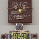
Step 12: The Feedback Resistors

The feedback input of the TPS63000 has to be fed a voltage of 500 millivolts derived from the output. With a 5 volt nominal output, this means a division ratio of ten or two resistors, one nine times the other.
Ransacking all my surface mount boards (in my junkbox) threw up the pair you see in the figure. They were connected together as shown, then connected to a battery and my trusty multimeter verified that the division ratio was indeed ten.
If you are confused, on the left is a 523K resistor ie, 5, 2 and 3 followed by three zeroes, in ohms. On the right is a 4.7 Megohm resistor, ie, 4 and 7 followed by five zeroes, in ohms.
47 divided by nine is approximately 5.23.
Step 13: The Resistors in Place

The resistors have been soldered into place, though due to limitations of space they had to be stuck upright to the output capacitor.
The whole thing is held together with liberal applications of superglue - otherwise the solder joints might come apart each time the board fell off the table.
Now all that remains is for the inductor and input capacitor.
Step 14: Niche for the Capacitor, Too.

I decided to cut into the board for the input capacitor, and use solder pins for the input connection.
The outline of the capacitor has been marked on the board for cutting out.
Step 15: Capacitor Trench

The capacitor trench is ready for use.
Step 16: The Finished Board

The board is finished, all components are in position.
It was tested.
First with two rather weak penlight cells - I did not trust my handiwork that much - and the output was 5.04 volts
Elated with the success, I tried it with three good cells - an input voltage of 4.5 volts - and the output was still 5.04 volts
Then I tried the voltage from the USB port of my computer - around 5 volts, though liable to jump around on the lower two digits - and still the output held steady at the same old 5.04 volts.
So it would seem that this thing works, at least during preliminary tests.
According to the datasheet it will start at 1.9 volts and accept a maximum of 5.5 volts, and hold its output voltage steady.
It is a buck - boost converter, which means it can accept input voltages above and below its output voltage, switching between modes automatically in order to keep the voltage steady.
It could be fed from a rechargeable cell in order to maintain the USB supply voltage even when the cable is disconnected from the computer - if that is any good.