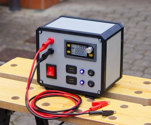
Introduction: Altoids Tin Speaker


Yet another Altoids tin speaker project. The speaker, circuitry, a single AA battery and 3.5mm male-male audio cable all fit together in the tin. Power is supplied with a Maxim MAX756 chip with circuitry right from the datasheet (see also the MintyBoost! both here and at ladyada.net) and amplification with an LM386 op-amp chip with circuitry again right from the datasheet (inspired by Make Magazine's Crackerbox Amp).
Anyone undertaking this project should have access to standard tools -- pliers, diagonal cutters, wire cutters and strippers, soldering iron and solder, multimeter, electric drill and brad point bits (more on these later). Experience making PCBs is also required.
Break Out of Your Pod -- Low Fidelity Audio -- High Fidelity Cool
Pictures
Several early commenters have noted the lack of pictures. There are now pictures detailing the preparation of the Altoids tin, battery holder, speaker, switch, audio jack, audio cable, and overall installation of parts and final assembly. There are also several pictures of the board with all of the electronic components installed but there is not a step-by-step walk through of this process. The main image for step 5 (Soldering Parts to PCB) has image notes identifying each of the parts.
If there are any additional pictures that you think would help the construction process, please let me know.
Step 1: Parts
Parts can be obtained from any of a number of electronic suppliers. Substitute as seems reasonable. The only crucial components are the speaker (because it fits so nicely into the tin) and the Maxim MAX756 and LM386 chips (because the board is designed for them). The links following the parts are to DigiKey and All Electronics.
Integrated circuits
1 x U1 -- LM386 audio amplifier DIP -- LM386N-1-ND
1 x U2 -- MAX756CPA DC/DC 3.3/5V DIP -- MAX756CPA+-ND
2 x Ux -- IC socket 8-pin DIP -- A32878-ND
Resistors
1 x R1 -- 10� 1/4W �1% metal film -- 10.0XBK-ND
Capacitors
1 x C1 -- 0.01�F -- 399-4150-ND
1 x C2 -- 0.047�F -- 399-4189-ND
2 x C7, C8 -- 0.1�F -- 399-4151-ND
3 x C3, C5, C6 -- 100�F -- P5152-ND
1 x C4 -- 220�F -- P5153-ND
Inductor
1 x L1 -- 22�H radial -- M9985-ND
Diode
1 x D1 -- 1N5818 Schottky 1A 30V -- 1N5818-E3/1GI-ND
Miscellaneous
Speaker 8�� 1/2W 57mm square (1) GF0576-ND
Battery Holder 1-AA 6" wire leads (1) 2461K-ND
Phone jack stereo 3.5mm (1) MJW-22
Audio cable 3.5mm male-male 12" (1) CB-400
Toggle switch SPDT 1/4" on-on (1) MTS-4
Image of all parts together with image notes identifying each part
Step 2: Schematic and PCB Layout
As noted in the introduction, the circuitry surrounding the Maxim MAX 756 and LM386 chips is directly from their respective datasheets. The schematic and the PCB were designed using the freeware version of the EAGLE Layout Editor from CadSoft.

Step 3: Making and Preparing the PCB

There are numerous resources on the Internet that describe the process of creating PCBs.
Transfer
I had (and still have) considerable difficulty getting consistent transfers onto the copper board. I currently use Press-n-Peel Blue Transfer Film from Techniks.com. I have also tried following the process detailed by riccibitti with little success (my impatience). It seems as if everyone has a preferred and flawless method, and none of them work well for me! I end up using a Sharpie to fill in the mask. This is overall the weak link in the making of PCBs.
Etching
After several frightening attempts at etching with Ferric Chloride over a pan of warm water in my kitchen, I moved into a chemistry lab and used the technique described in the Instructable Stop-using-Ferric Chloride. The materials were cheaper, more readily available (local hardware store and CVS), cleaner and safer. The initial etching was fast and aggressive, although I had some trouble with subsequent batches.
Cutting
I don't have a good method for cutting PCBs. Suggestions and recommendations would be appreciated.
Drilling
To drill the holes I used a Dremel tool with drill extension and a 1/32" bit for most holes. For the diode and holes for the speaker, battery, switch, and audio connection, I used a 3/64" bit. Bits are from Lee Valley.
Step 4: Preparing the Altoids Tin


The tin needs two sets of holes. I use a metal punch to mark the hole locations and brad point bits (for wood) to drill the holes. The brad point bits have a center point and two cutting edges. They won't skate and the edges cut slowly through the metal. Brad point bits are available from Lee Valley (among other places).
The first is a set of 1/8" holes directly over the speaker in the pattern of your choice. I mark out the pattern on 6 x 6 graph paper and tape the paper onto the lid of the tin roughly located over the speaker. In order to prevent pushing the top of the tin in, support the inner part of the lid on a small block of wood when punching and drilling the top. With the paper and wood in place, I dimple the tin using the punch. When drilling, go slowly at first. The cutting edges of the brad points should make an even circle. Drilling with the bit anything but perpendicular to the surface may result in the bit grabbing and tearing the metal.
The second set consists of two 1/4" holes on the left side of the tin for the switch and audio jack. Space these fairly wide but so far apart that they fall on the curved part of the tin. Center them vertically on the portion of the side visible when the lid is closed. Mark with punch and drill very carefully. The caution about the bits grabbing the tin applies more strongly with the bigger bits.
Step 5: Soldering Parts to PCB


There are numerous resources on the Internet that describe the process of soldering electronic components to PCBs. See, for example the soldering tutorial at ladyada.net. The order in which you install components doesn't really matter, although I have found working from smallest to largest them easiest. I assemble the board in the following order.
Jumpers
I use jumpers (small pieces of wire) in a few places instead of having a double sided board. There a several places in this design where I could not figure out a simple way of getting a wire from one place to another without crossing a second wire. Jumpers were my solution.
Note that the schematic calls for a second diode (D2) where power enters the LM386 chip. This was necessary when the circuit only consisted of the amplifier portion; I don't think it is necessary any more and I replace it with a jumper.
Chip holders
I put the chip holders in next. The two provide a relatively stable surface on which to balance the board upside down for future soldering. The orientation of the chip holders matters -- make sure the notched end is located as illustrated so that the chips are oriented correctly when inserted.
Small capacitors
The four small capacitors go in next.
Resistor
The resistor is positioned vertically
Diode
The holes for the diode should be 3/64. The spacing between holes is a little small so care must be taken fitting the diode in place. More important, however, is getting the orientation of the diode correct.
Large capacitors and inductor
These go in easily and form a sort of wall to support the battery holder. Care must be taken to ensure the correct orientation of the electrolytic capacitors. Note the location of the white strip on each capacitor. The orientation of the inductor does not matter.
Check your work
Be careful to orient the components properly. The orientation of the chip holders, the electrolytic capacitors and the diode matter. Check the layout diagram and the schematic or just make sure things match up with the pictures!
Attachments
Step 6: Preparing the Battery Holder


To protect the leads on the battery holder, slide a small piece of 1/16" heat shrink tubing into the holes through which the leads exit the holder. The battery holder barely fits into the tin and the heat shrink tubing protects the leads from abrasion. The orientation of the battery holder in the tin is chosen to keep the long lead on the component side of the tin.
Clamp the two wires together at the upper end of the holder with a short piece of 1/8" heat shrink tubing. Cut the end of the heat shrink tubing at an angle to get a closer fit to the holder.
Use diagonal cutters to cut the two tabs that hold the battery in. This will make replacing the battery considerably easier once everything is assembled
Step 7: Preparing the Speaker


The rounded corners of the speaker do not fit nicely into the corners of the Altoids tin. Use diagonal cutters to cut away at the two left corners and increase the radius of the curve. Before assembly, check that the speaker fits snuggly under the left hand lip of the tin.
When soldering, loop the wires through the holes in the lugs for extra reinforcement. Add pieces of 1/16" heat shrink tubing to prevent abrasion. Note that the wires go to the left when the speaker is upside down and will go correctly to the right when the speaker is right side up in the tin. Note that the red wire is above the black wire.
Step 8: Preparing the Switch

Thread the wires through the holes in the lugs and solder and reinforce the connections with 1/16" heat shring tubing. If this tubing does not fully cover the lug, slide a additional piece of 1/8" tubing on down to cover the lug and solder connection. Clamp the wires together with a short piece of 1/8" heat shrink tubing.
Cut the extra lug off the DPST switch if necessary (it may contact the bottom of the speaker and is not used in this project).
The wires need to be bent twice in order to fit around the speaker. They should follow the walls of the tin. Note that the red wire is above the black wire.
Step 9: Preparing the Audio Jack


This is the most complicated piece to make. Start by straightening the lugs with a pair of needle nose pliers. Then bend any terminals that are part of an integrated switch out of the way.
Join the left and right signal lugs with a small piece of wire. This is supposed to merge the left and right signals from the input device -- I hope it does! This one of the trickier solders. I carefully cut a piece of (green) wire to length, strip the ends and bend it fit exactly. Once I have a good fit, I flow a bit of solder onto the lugs, position the wire, and then melt the solder and push the ends in place. Usually I burn my fingers. You have to work quickly and be careful not to melt the switch.
Note the orientation of the audio jack in the tin. I have the input wire (red) coming of the top lug and the ground wire (black). Solder wires to two lugs on the switch and reinforce the connections with heat shrink tubing. Clamp the wires together with a short piece of 1/8" heat shrink tubing. Note that the red wire is above the black wire.
The wires need to be bent back and follow the walls of the tin.
It is a good idea to do a continuity check at this point. Plug in the cable and make sure that the two signal wires connect and the ground connects to ground.
Step 10: Preparing the Audio Cable


The ends of the audio cable are fragile and need to be protected with heat shrink tubing. Cover each end of the jack with 1/4" heat shrink tubing.
Step 11: Installing Additional Parts


Cut the leads of the external parts to length one at a time by fitting the board into the tin and placing the part over it. Too long is better than too short. Solder them into place in the following order -- switch, audio jack, battery holder, speaker.
Step 12: Testing the Circuit
Before the final assembly, it is a good idea to check the circuit. Make sure that the two chips are in and a properly charged battery is installed in the correct orientation. Turn on the Altoids Tin Speaker and hope for the best. You should hear a faint hum from the speaker. Attach a noise-making device. Hopefully, you will hear music.
Troubleshooting? You are on your own.
Step 13: Final Assembly
Cut a piece of heavy cardboard (I use either pieces of picture framing mat board or cardboard beer coasters) to fit inside the bottom of the Altoids tin. The radius of the corners of and Altoids tin may be approximated by a quarter. This piece insulates the board from the metal tin. Note that in order for the 3.5 male-male audio cable to fit in the tin, this piece must not extend all the way to the right side of the tin. It should be sized to fit under the entire circuit board.
Insert and attach the audio jack and switch first. To do this, fold the speaker up and out of the way. Then slide the board into the tin and push the threaded portions of the audio jack and switch through their respective holes. Tighten.
Fold the speaker down into place. You will have to push the long sides of the tin out a bit to get the flange of the speaker to snap in place under the rolled edge of the tin. Slide the speaker all the way to the left. If it does not fit under the left-hand rolled edge, trim the two corners a bit more.
While the sides of the tin are still splayed out, slip the battery holder into place. Be careful not to abraid the leads. Note that the battery holder is positioned so that its red lead runs up the side next to the electronic components.
Straighten the sides of the tin and make sure that the flange of the speaker is seated underneath the rolled lip of the tin.
Add a battery, close up the tin, and enjoy!
Step 14: Controlling Gain -- Easy Way
The gain of the LM386, as the ATS is currently constructed, is set only to 20. The effect of this is that the ATS is not terribly loud. I found that to get desired volume, I had to turn up the volume of my MP3 player almost to its maximum level. This distorted the signal and sound from the ATS, and, poor speaker aside, result in very poor sound. The amplification of the system should take place in the LM386 (where it belongs) and not in the source providing the signal.
Careful examination of the PCB will reveal two pads just above pins 1 and 8 of the LM386. By joining these two pins with a piece of wire, the gain will be set to 200 and the ATS will be considerably louder. The datasheet for the LM386 indicates a 10uF capacitor should join these pins and that pin 7 needs a bypass capacitor. I have not noticed any problems with a simple wire.
This is the easy way to modify the gain. A more elegant and complicated approach is detailed on the next page.
Step 15: Controlling Gain -- Elegant Way
The gain of the LM386 amplifier chip is controlled by a resistor (and capacitor) between pins 1 and 8. I replaced the toggle switch with an ALPS RK097 10K ohm stereo audio taper potentiometer with power switch from Tangent's Parts Shop (and available nowhere else, it seems). I used one of the two potentiometers to control the resistance between pins 1 and 8 on the LM386 and the power switch to control the power.
The effect of this change is that with the gain turned all the way up (resistance as low as possible), the ATS is quite loud and with the gain turned all the way down (resistance as high as possible) the ATS is somewhat louder than with no modification at all. In any case, both the easy and elegant modifications place the burden of amplification on the LM386 and the sound is considerably better at higher volumes.