

Introduction: Arduino Programmable Constant Current Power Resistance Dummy Load
Glad to see you have arrived on this page to learn how to build a programmable constant direct current dummy load. This load will allow you to draw a set current from any source. This load can also be set to a constant resistance or a constant power.
I have been working in the Electrical Engineering field for quite a while now with my studies mainly focused on power. I have always had in interest in electronics but I had never really kicked off until a few years ago when a mate of mine said, "Have you seen an Arduino?". I'm the sort of person that learns by trying stuff, stuffing it up and then fixing it. I tend to be a perfectionist so it takes me a while but I am quite often happy with the result!
One of the first things any good electronics lab needs is a power supply, so me being me thought I would build one! who wants to buy one when you can make one. As this is quite a project for my first attempt, I thought that a dummy load would be a good start as the technology and principles are very similar. My inspiration for this project started by watching Dave Jone's EEVBlog (Electrical Engineering Video Blog) and he did an episode on one that he had done.
That's where this project started and grew as the project went on! Please check out this project and please leave your feedback at the end.
Lets get started!
Step 1: System Specifications
This dummy load has the following specifications:
- Maximum Input Load Voltage - 24V
- Maximum Input Load Current - 8A
- Maximum Input Power Dissapation - 50W
- Operating Voltage - 5V
- Power Source - USB or External Power Pack (5V)
- Minimum load current draw - 15mA - Due to op-amp offset.
- Load Current error - Up to Approximately 3mA.
Step 2: How It Works

Don't let the intro image scare you! I explain it all in this step.
If you're new to electronics and electrical theory in general, this step will guide you through the theory behind it, how it works and why. If you have been doing electronics for a while then it may be worth skimming over this article just to refresh your memory and see what principles are used.
Most electrical theory falls back to good old Ohm's Law,
V = I x R
V = Voltage I = Current R = Resistance
And this dummy load is no different, in fact, there is only one other formula used in this whole project, and that is,
P = V x I
P = Power V = Voltage I = Current
That's it! pretty easy really.
The way that this dummy load works is that it uses a MOSFET (more on MOSFETS in a minute) as a big "variable resistor" to control how much current is let through the system. By sensing a voltage and feeding that back to the MOSFET via an op-amp (more on op-amps later also) it knows how much current its letting through and adjusts its internal resistance accordingly to maintain the current it's supposed to be letting flow. If that sounds a bit confusing, stick with it and it will make more sense as we go on.
The flow of electricity can be closely compared to the flow of water, think of the voltage as the pressure of the water, the higher the pressure the more you can do with it, for example, a high pressure water cleaner, will clean much more dirt and use much less water than a garden hose doing the same job. Think of current as the flow of water, the more water you have flowing the faster you can fill the bath. Think of resistance as a kink in the hose, when you put a kink in the hose you need a much higher pressure (voltage) to push the same amount of water (current) through the kink. Think of power as the bath tub, regardless of your water flow (current) it will still take the same amount of water (power) to fill the bath tub, the faster the flow (higher current) the faster it will fill and vice-versa. In our dummy load, the key component is the kink in the hose, the MOSFET. We need to control that resistance (kink) to maintain the current (flow) at our set value, regardless of the input voltage (pressure).
You may be wondering what a MOSFET is or what it is used for. A MOSFET is like a variable tap, we can send a voltage to it, known as a gate voltage, and this changes how wide open the tap is. There are two main types of MOSFETs, an N type and a P type. This article does a very good job of explaining the difference between the types and what they do. This load uses an N type MOSFET to control the current. In general, A MOSFET has three pins, the gate, drain and source. The drain and the source can be though of as the hose and the gate is like the tap valve. In the case of an N type MOSFET conventional current flow is from the drain through to the source, I know that seems a little confusing but it is because of the actual electrons flow, we won't get into that here as it can confuse you! Lets just consider conventional current flow for now. In the case of our N type MOSFET, the higher the gate voltage the wider the tap is open, the closer to 0 V the closer that tap gets to closing.
As you can probably imagine we need to adjust that resistance (kink) very quickly to ensure our current is as stable it can be. Because of this, we can't rely on the microprocessor to sense the current, calculate what the current should be, calculate what the resistance should be to get that current, convert that to a voltage the MOSFET needs to be set at that resistance then send it to the MOSFET. Way too long! Way too unstable! To over come this issue we bypass the micro controller all together and use an op-amp to do all the hard work!
Before we get onto the op-amps we need to cover one more aspect of the circuit and that is those 10 resistors next to each other R1 - R10. They are 10 x 1 ohm resistors in parallel, parallel resistance can be a little confusing to calculate the total resistance of that section, however, considering they are all the same value we can cheat a little, we can divide the value of 1 resistor by how many are there, in this case, it is 1 divided by 10, or 0.1 ohms, If you where to put a multimeter across those resistors it would read 0.1 ohms, this is known as the sense resistor. Why 10? why not just 1 0.1 ohm resistor? Well for three reasons.
- Accuracy
- Power Dissipation
- Cost
The reason we have improvement in accuracy is because that 10 resistors in parallel will tend to even each other out in their errors and end up with a more precise resistance value than if you used 1 x 0.1 ohm resistor. One thing we haven't really looked at is power. As current passes through a resistor it drops voltage (drops pressure as it passes through a kink) this drop in voltage is known as power dissipation, power can be many things, in this case, its heat. Many things rely on heat off resistors, your kettle, bathroom heater, hair dryer, hot water service and the list goes on. In this case, its an unfortunate by-product. However, lets just do a few quick calculations on how to calculate just how much power is there. This load is capable of carrying 8 amps, lets first work out how much voltage we will drop across our sense resistor of 0.1 ohms,
V = I x R
= 8 x 0.1
= 0.8 volts
Now we know how much our voltage dropped we can work out our power dissipation
P = V x I
= 0.8 x 8
= 6.4 watts
Let me tell you, that's quite a lot of power dissipated from one resistor! Which brings me to the other element, cost, one 0.1 ohm resistor with a 1% accuracy that can dissipate 6.4 watts is in the order of $7 - $10 just for one resistor where as 10 x 1 ohm resistors that can dissipate 1 watt each are $0.30 each.
The purpose of these sense resistors is it allows us to accurately measure the current in the circuit against a known resistance, no mater what, ohms law always applies, as we have shown, if there is 8 amps going through a resistance of 0.1 ohms, there will always be a voltage drop of 0.8v. Like wise, if we put 1 amp through the 0.1 ohm resistor we will get a 0.1v drop, always. Try it, put any value of current into the above formula and you will get a proportional voltage drop across those resistors. Remember this, we will see why that's important in a little while.
OK, Op-Amp time! Op-Amps can be very complicated beasts and we are certainly not going to cover all aspects of the op-amp in this instructable. If you wanted to read a bit more into the op-amp then this is a very good tutorial to explain them in detail. For this project I have used an LM324 which is one chip that has 4 op-amps inside, the op-amp we are considering at the moment is shown in the image above as U2a - LM324a.
On most op amps there are 5 pins, a non inverting input (pin 3), an inverting input (pin 2), an output (pin 1) and a power supply (pins 4 and 11). One important property of the op-amp that we need to consider is that it will do everything it possibly can on the output to try and keep the inputs at the same voltage. The op-amp hates having a difference of voltage on the input. In fact this is very important to understanding the inverting and non-inverting amplifier circuits.
The dummy load makes use of this very useful feature of the op amp to control the MOSFET gate (the kink in the hose) so that it can keep the current to the level we set. How does it know what the current is? By reading the sense resistor. Let's have a look at that for a minute, in the image above, the sense resistors are R1 to R10 in parallel, as we have described the sense resistor will drop a voltage that is proportional to the amount of current flowing through it, as the very next connection in the circuit is ground (or 0 volts) ohms law says that if we have 1 amp flowing through the sense resistors that they will drop 0.1 volts. That means, if we have 0.1 volts at the top of the sense resistors and 0 volts at the bottom then we must have 1 amp flowing!
We are finally getting to the fun part! Now, if you have a look at the circuit above, the top of these resistors feed back to the inverting input of the op-amp (It does go through a few other resistors and capacitors but please ignore them for now, we will talk about them in another step, trust me when I say, that 0.1 v will be fed back to the inverting input). You will also notice that the gate of the MOSFET (M1 - BUK954R8-60E) is connected to the output of the op-amp. Going back to what we said earlier, that the op-amp will do everything it can on its output to keep its inputs the same, so with that in mind, if we set a voltage of 0.1 volts on the non-inverting input of op-amp, it will do everything it can on its output to get 0.1 volts on the inverting input. So, it will put as much voltage as it has to on the gate of the MOSFET (opening the tap) to open it enough so that 1A flows. Likewise if we set 0.8 volts on the non-inverting input, it will do everything it can on the output to get 0.8 volts on the inverting input. That is how it works, what ever voltage you set, it will drive the MOSFET enough to get the same voltage on the other input. It's as simple as that!
Step 3: The Whole Picture
In the previous step I covered some basic electrical theory plus a broad overview on how the load works.
Well, now you know how it works, I am guessing you want to know how everything fits together. Its all well and good to have a system that can draw a constant current but if you have nothing to control it with and see what's going on then its really not very good is it!
This is a quick overview of the components in the project and how they fit in. I will explain everything in more detail in separate steps. I have also attached the final schematic to help you along the way.
- MOSFET - M1 - BUK954R8-60E - The MOSFET is used to control how much current is let through the load path.
- Op-Amp - U2 - LM324 - The op-amp is a quad op-amp and is used in various parts of the circuit, its main function is to control the MOSFET.
- ADC - U3 - MCP3204-CI/SL - The ADC (Analogue to Digital Converter) has 4 inputs and converts an analogue voltage into a digital binary number that can be understood by a micro-processor.
- DAC - U4 - MCP4922-E/SL - The DAC (Digital to Analogue Converter) has 2 outputs and converts a digital binary number into and analog voltage. This is used to set the load current and the cooling fan speed.
- Voltage Reference - U1 - ADR380ARTZ - The voltage reference is used by the ADC and the DAC to convert voltages to binary numbers and vice versa.
- Temperature Sensors - U6 & U7 - LM94022BIMG - These sensors are used to measure the temperature of the heat-sink attached to the MOSFET.
- Fan - FAN1 - EB50100S2-0000-A99 - The fan is used to cool the heat-sink.
- Processor - U8 - ATmega32U4-AU - The processor brings everything together, it is based on the Ardunio Leonardo design.
So, that's about everything that's in it, not really a complicated design but they all compliment each other.

Step 4: BUK954R8-60E - MOSFET

Probably the most important component in the whole design is the MOSFET, this dummy load uses the BUK954R8-60E N type MOSFET - datasheet.
A MOSFET if very similar to a transistor with one major difference, the MOSFET is a voltage controlled device and a transistor is a current controlled device. You can think of the MOSFET (as with a transistor) as a hose with an in-line valve. By controlling this valve you can determine how much current is let though the hose, with N-type transistors, the higher the current you apply through the valve the more current it will let flow through the hose, with N-type MOSFETs, the higher the voltage you apply to the valve the more current it will let through the hose.
That's enough on transistors, lets focus on the MOSFETs and getting the terminology correct. A MOSFET usually has 3 pins,
- Source
- Gate
- Drain
The image above shows the circuit symbol for the N-channel MOSFET. Conventional current flows from the Drain to the Source (this is the hose) and is controlled by the gate (this is the valve). As the gate has a very high input impedance (similar to resistance) virtually no current flows into the gate when it has a voltage applied to it. This makes it fantastic for driving directly from an op-amp or micro-controller as it doesn't draw any current from the device controlling it, unlike the transistor that does take current and can overload either the controller or the transistor, this is why you often see a "base resistor" with transistors. This property of the MOSFET having a very high gate impedance means that the gate is basically a large capacitor, this can cause problems which we will investigate in another step.
There are some important properties when comparing different MOSFETs that we will now look into,
- Vds - drain-source voltage - This is the voltage across the drain and source pins when the MOSFET is turned off.
- Id - drain current - This is the current that flows through the drain and source pins.
- Ptot - total power dissipation - This is how much power the MOSFET can dissipate.
- Rds on - drain source on resistance - This is how much resistance the MOSFET has when it is fully on.
- Vgs(th) - gate source threshold voltage - This is how much voltage has to be applied to the gate before the MOSFET starts to allow current through.
There are many more things to consider but these are definitely the most important ones for this project.If we think back to our system specifications, our maximum load input voltage is 12V, this will represent Vds when the MOSFET is turned off, the max Vds for this MOSFET is 60 volts, as per table 1 in the datasheet. Our maximum input current is 8A, this will represent Id, the max Id for this MOSFET is 100A as per table 1 in the datasheet. Our maximum power dissipation is 50W, this will represent Ptot, the maximum Ptot for this MOSFET is 234W as per table 1 in the datasheet. As you can see, our project is well within the limits of this MOSFET, as a side note, it wouldn't be advisable to push any product to its limits.
This leaves the Rds on and the Vgs(th), Rds on isn't that critical for this project as the MOSFET will nearly never be turned all the way on. The Vgs(th) is the main property that led me to choose this MOSFET, for this particular application, it is very important to have a MOSFET that starts to conduct at a low gate voltage, why you ask? Because we are driving this MOSFET with an op-amp that has a supply voltage of 5 volts and hence max output voltage of 5 volts (or close to). So we need this MOSFET to be conducting all of the current we want with a gate voltage of less than 5V. It can be quite difficult to find a MOSFET that will allow this much current through with a gate voltage of less than 5 volts, they are quite often in the order of 10 or 12v. A MOSFET that conducts at lower gate voltages is often called a logic level MOSFET.
Another very important thing to consider is the total power dissipation of the MOSFET and how hot it's going to get. As we discussed in step 1, every time you have a current passing through a resistor it drops voltage, when there is a voltage drop in this situation there is power dissipation, in other words, that energy that is lost as the voltage drops is converted to heat and dissipated through the MOSFET. We can basically consider our MOSFET as a kind of variable resistor, this allows us to calculate how much power it will dissipate. Lets consider a 12 volt input and we have set our current to 4 amps, for ease of calculation lets consider that the whole 12V is dropped through the MOSFET (of course we do drop some voltage in the sense resistors but lets not make our life difficult at this stage). To work out the power dissipated we use this formula again,
P = V x I
= 12 x 4
= 48w
So, that's where you may compare that to the datasheet and think, "yep, its under the 234w we're right!" Unfortunately its not that easy, there is one very important factor that we need to consider, how hot will it get? we can head to the datasheet and find the Rth(j-a) - Thermal resistance from junction to ambient - This value tells you how much this device will rise in temperature when mounted free standing in still air. This device will rise 60K/W as per table 5 in the datasheet. Which is 60 degrees Kelvin per watt of power dissipated, that is also the same as saying 60 degrees Celsius per watt, Kelvin is sometimes used as its an absolute value. So lets do the maths, if we are dissipating 48 watts, we will rise 48 x 60, that's 2880 degrees! that will cause the magic smoke to escape and could be very dangerous! To prevent this from happening we need a heat sink, a big one!
Thermal resistance isn't that hard to work out but there are many things to consider, Dave Jones does a fantastic job of explaining it in this video, I would suggest watching it if you can.
I have used the Aavid Thermalloy OS518-100-B heat sink in this project which is 100 mm wide and reduces our temperature rise to 2.22 degrees Celsius per watt in still air, this now takes our heat rise for our maximum power dissipation of 50 watts to 2.22 x 50 = 111 degrees Celsius, much more respectable!
So that covers the design decisions made in choosing the MOSFET.
Step 5: LM324 - Op-Amp


The LM324 (datasheet) is a quad op-amp that we use for various different tasks within the project, lets have a look at them.
The first and most important function of our op-amp is to drive the MOSFET as described in a previous step, a voltage is applied to the non-inverting input of op-amp a, lets consider 0.1v, then the output of op-amp a will do what it has to, to make the inverting input equal 0.1v which is connected to the top of the sense resistors, that gives us our constant current. If you haven't read that step, I suggest checking that out. As I also mentioned, there are a number of other resistors and capacitors hanging around that may cause a lot of confusion, that has to do with a property of the MOSFET that I also mentioned, about the gate acting like a capacitor. Long story cut short, op-amps don't like driving capacitive loads, this is quite a complicated subject and can get very confusing very quickly, if you wish to read more into it then this is a great article that describes how an "ideal" op-amp has zero output resistance but a real op-amp does have some output resistance, when driving a capacitive load this turns into an RC circuit that can oscillate wildly when the phase loop is not stable. Resistors R15 and R16, also capacitor C3 make this loop stable for this op-amp and MOSFET.
The remaining 3 op-amps in our circuit are used as buffers, the purpose of a buffer is to stop any current flowing from or into a section of a circuit that isn't designed to do so. Because an op-amp has a very high input independence they draw very little current from the portion of the circuit they are connected to. A buffer is wired as shown in the second picture above and can be considered as an amplifier with a gain of 1, if we go back to our earlier property of an op-amp, that it will do what ever it can on its output to make both inputs equal, in the case of the buffer, the output is connected directly to the inverting input of the op-amp, so whatever voltage you apply to the non-inverting input of the op-amp it will drive its output so it equals.
Lets look at them in circuit, U2b and U2c can be shown next to the ADC, they are acting as input buffers. U2b is sensing the input load voltage ADC-VIN which is measured up near the MOSFET and U2c is measuring the voltage at the sense resistors ADC-IOUT, so the system can check the output current to see that it is what its supposed to be. As both of these points in the circuit would be more than happy to give me all the current I want, whether I "want" it or not, this leakage current can cause issues when we have set our load current to very low levels, if we have set our load current to be 5mA and we are using 5mA just to read the voltage, we are effectively drawing 10mA from our load not 5mA as we have set it, we need to stop this current escaping from that part of the circuit by buffering it and just passing the voltage through to the ADC to be measured.
Now we can look at another use for a buffer, U2d is being used as a buffer to drive the fan, the fan is speed controlled through a transistor, to drive this transistor fully can take quite a lot of current. The DAC that's setting the voltage to control the fan speed cannot supply enough current to run the transistor properly, so we send this voltage to the buffer and then it drives its output at the same voltage but can supply much more current. Both very good uses for a buffer.
Step 6: MCP3204 - ADC

An ADC (Analogue to Digital Converter) helps us read an analogue voltage and convert it to a digital binary number that allows the micro-controller to under stand it. This MCP3204 (datasheet) ADC is made by Microchip and uses an SPI interface to communicate with the Micro-controller. I will talk more about the SPI later on in another step.
The pins for the MCP3204 are as follows,
- Input for ADC Channel 0.
- Input for ADC Channel 1.
- Input for ADC Channel 2.
- Input for ADC Channel 3.
- Not connected internally.
- Not connected internally.
- Digital ground - This project uses a common ground.
- This is an active low Chip select pin used for the SPI interface (explained in a later step).
- This is data in, sometimes known as MOSI used for the SPI interface (explained in a later step).
- This is data out, sometimes known as MISO used for the SPI interface (explained in a later step).
- Serial clock pin used for the SPI interface (explained in a later step).
- Analogue ground - This project uses a common ground.
- Voltage reference input.
- Vdd - Supply voltage pin - 5V
Strictly speaking, I didn't really need to include a separate ADC in the design as the ATMega32U4 has an inbuilt 10 bit ADC, however, there are two main reasons I did,
- Better resolution
- Because I wanted to play with one!
As you probably already know micro-controllers are digital, digital products only work on 0s and 1s. A digital device, by itself, cannot read an analogue value like a voltage or 3.21V. Digital products can only read logic level values, for example, 0v "it's off", 5v "it's on".
Before we get too far into this, a little on what binary is, binary is a base 2 numbering system, that means it can only count 2 steps before ticking over to the next digit.
0
1
Our normal numbering system, the decimal system, is a base 10 numbering system, we can count 10 steps before ticking over to the next digit.
0
1
2
3
4
5
6
7
8
9
Here is an example of what 0 to 7 looks like in binary,
0 0
1 1
2 10
3 11
4 100
5 101
6 110
7 111
Each digit is known as a "bit" and 8 bits is a "byte" so the maximum decimal number you can count to using an 8 bit binary number is 255. So that is 256 different values because we include 0 as a value.
0 0
.. ..
.. ..
255 11111111
The resolution of an ADC represents how many bits or steps of a binary number it can measure an analogue value and convert it to digital binary number, for example,
- 8 bit ADC can measure 256 steps = 2 to the power of 8
- 10 bit ADC can measure 1024 steps = 2 to the power of 10
- 12 bit ADC can measure 4096 steps = 2 to the power of 12
I'm guessing this isn't making much sense yet, that's OK, it will.
All ADCs have to use a reference voltage, this reference voltage allows the ADC to compare the voltage its reading against the reference voltage and return a percentage as the binary number. OK, example time, for an 8 bit ADC, the maximum number of steps it can break the reference voltage up into is 256 (dont forget 0V), so for ease, lets make our reference voltage 255v (it wouldn't be but lets just go with it), if the voltage the ADC reads is 255v, it compares it to the reference voltage and says, OK its 100% of my reference voltage so im going to send you the highest digital value I can, 255. It reads it again and its now 128V, it says OK, its now only 50% of my reference voltage so I will send you 50% of my binary value, 128.
For our example earlier, we had a reference voltage of 255V and we had 256 steps, so that's easy, it can read in 1V increments, what if we needed to read 0.1V increments? Well that's just tough, because an 8 bit ADC can only count to 256. That's where a higher resolution ADC comes in. Now lets compare against a 100V reference voltage so we can see the benefits of using an ADC with a higher resolution.
8 bit = 256 steps, we divide our reference voltage by our resolution to find out what voltage differences our ADC can read, 100 / 256 = 0.39V. So the lowest our 8 bit can read is 0.39V, then the next value will be 0.78V
10 bit = 1024 steps, 100/1024 = 0.098V. So the lowest our 10 bit can read is 0.098v, then the next value will be 0.196V. Much much smaller gap between the readings.
12 bit = 4096 steps, 100/4096 = 0.024v. So the lowest our 12 bit can read is 0.024v, then the next value will be 0.048v and so on. Then there will be 4096 different values before it reaches the full 100V.
As you can see, its a much much better accuracy the higher resolution you go.
Step 7: MCP4922 - DAC

A DAC is basically the opposite to an ADC, you send it a digital binary number and it converts it to an analogue voltage. The DAC I have chosen for this project is also 12 bit MCP4922 DAC (datasheet) made by Microchip and also uses an SPI interface to communicate.
The pins for the MCP4922 are as follows,
- Vdd - Supply voltage pin - 5V.
- Not internally connected.
- Active low chip select used for the SPI interface (explained in a later step)
- Serial clock used for the SPI interface (explained in a later step)
- Data in, sometimes known as MOSI used for the SPI interface (explained in a later step)
- Not internally connected.
- Not internally connected.
- This is used to latch the data into the DAC, we don't use this function so the pin is permanently tied to ground.
- This is used to shut-down the DAC, we don't use this function so the pin is permanently tied to 5V.
- Output of DAC channel 1.
- Input for the Voltage reference.
- Vss - Ground
- Input for voltage reference.
- Output of DAC channel 0.
The principles of operation are very similar to the ADC, if you aren't familiar with the binary numbering system or haven't read the previous step, then I would suggest checking that one out first.
The DAC also relies on a reference voltage to assist in converting the binary number to an analogue voltage. It will convert the binary number to a percentage of the analogue reference.
If we go back to our earlier example used in the ADC with a reference voltage of 100V. If we send the binary equivalent of "1" to an 8 bit DAC it will output 0.39V as that's the lowest percentage of 100V its able to output, if we send the binary equivalent of "2", it will output 0.78V and so on until we send it a binary equivalent of "255" it will output 100% of its reference voltage which is 100V. Lets consider the 10 and 12 bit DACS,
10 bit - Send a "1" it will output 0.098V, send a "2" it will output 0.196V, send it a 1023 it will output 100V.
12 bit - Send a "1" it will output 0.024V, send a "2" it will output 0.048V, send it a 4095 it will output 100V.
Again, the higher resolution the DAC the more precise you can control its output voltage.
This DAC has two outputs, output 1 goes to the non-inverting input of the op-amp U2a that controls the load current, output 2 controls the speed of the fan buffered through op-amp U2d.
Step 8: ADR380 - Voltage Reference

In the previous steps we have discussed using a voltage reference to help the ADC and the DAC to convert between analogue voltages and digital binary values, well this is it! In our examples earlier we spoke about using a reference of 100V, well that's certainly not an option, well for these chips anyway.
This ADR380 reference (datasheet) outputs a very stable and precise 2.048V to use as a reference, why 2.048v you ask? seems a weird number. Well there is a very good reason for that and it goes back to the number of bits resoloution, there is 4096 steps with a 12 bit device, 2048 is exactly half of 4096. So lets figure out what each step is worth using a reference voltage of 2.048.
2.048 / 4096 = 0.0005V or 500 micro volts, so, if you send a "1" to a 12 bit DAC using a reference of 2.048V its going to output 0.0005V, for every increase in step it will increase by 0.0005V, for example, if we send it a "2" it will output 0.001V and so on until we reach 4095 (remeber 1 less because 4096 steps includes 0) when it will output the full 2.048V. Much easier to do the maths and work out in programming and in the rest of your circuit.
Lets now convert this into practical use in the load, as we have learnt, if I want to set my constant current to the maximum of 8A, I will need to send 0.8V to the non-inverting input of op-amp U2a so that it will drive its output so the sense resistors will read 0.8V hence allowing 8A through the load. But hang on, we have just spend all this time explaining this DAC can give us all these steps all the way up to 2.048V now the maximum we can output in channel 1 to control the current is only 0.8V, what a waste. If you refer to the schematic, you will see resistors R17 and R18 near the input to op-amp U2a, this is a voltage divider that divides the input voltage by 2.5 before it goes into the op-amp, so if our DAC is outputting 2V, this divided by 2.5 equals 0.8V. Now we can use our DAC for almost the whole range!
Step 9: LM94022 - Temperature Sensor

This project uses 2 x LM94022 analogue temperature sensors (datasheet) to monitor the temperature of the heat sink attached to the MOSFET.
This allows us to control the speed of the cooling fan or shut down the unit if it gets too hot. The selection of these sensors was mainly based around their maximum temperature that they can sense to, as the maximum temperature the heat sink can get to has been calculated to be close to 120 degrees Celsius in still air, I wanted the temp sensors to be able to read up to 150 degrees without damaging the chip.
Both of the sensors are located under the heat sink one at either end, the board is designed so the base of the heat sink will sit on top of them and transfer the heat directly into the ship.
These sensors work by outputting a voltage proportional to the heat, this is almost linear which is nice! The pin out is as follows,
- GS0 - Calibration pin (see below description)
- Ground
- Output - This pin puts out a voltage that is proportional to the temprature
- GS1 - Calibration pin (see below description).
- Vdd - Supply voltage (5v)
GS0 and GS1 pins can be tied to a combination of Vdd and ground to set the level of voltage that is output. Check out the datasheet for more info. Ours is set that GS1 = Vdd and GS0 = Ground, this mode is referred to in the datasheet as GS=10, therefore if our sensor is at 25 deg C, pin 3 will output 1.831V and if our sensor is at 100 deg C, pin 3 will output 0.997V.
For more information on this and how the temp is calculated please refer to the programming step.
Step 10: EB50100S2-0000-999 - Fan


In order to keep the heatsink nice and cool I have installed an EB50100S2-0000-999 Fan(datasheet). It is 50 x 50 x 10mm and does quite a good job really.
This fan runs off 5V and does draw quite a lot of current when fully on, as there will be very few times that the fan will need to be fully on I have decided to speed control it. With modern fans there are many ways in which you can control their speed, including PWM and various other methods. The method I have used is purely analogue, the reason I chose this method is purely because I wanted to give it a go!
The PN2222 transistor (datasheet) is the key to how this all works (as a side note, be careful not to confuse this for the P2N2222, they have a different pin configuration and won't work, trust me!).
We spoke briefly how a transistor is similar to a MOSFET in its operation, it is like a valve in the hose. Before we talk about the differences in operation lets talk about the pins, in the second image you will see the schematic symbol, if we compare it to the MOSFET, the collector is similar to the drain, the emitter is similar to the source and the base is similar to the gate on a MOSFET. The main difference is, a transistor is a current amplifier, it accepts a current through the base which then travels through the emitter to ground. This current is quite small and is proportional to the much larger current it will then in turn let through the collector through to the emitter to ground also. There is obviously a limit to how much current you can put through the base leg of a transistor, this needs to be limited by the base resistor R25. I am not going to cover the selection and the operation of a transistor as much as I did for the MOSFET, however, this article and also this article cover it very well.
So, in short, we can control how much current the transistor will let through for the fan to operate by controlling the amount of base current we put through the transistor. As the base of the transistor is a fixed resistance we can control how much current is applied by changing the voltage applied. This is what the second channel on our DAC is for, if you remember, we discussed that an op-amp can be used as a buffer, that is exactly what U2d is doing for us. As a DAC cannot supply very much current to drive the transistor (approximately 15mA), we need to put its voltage into a buffer so the op amp can supply the base current instead. The DAC could probably do it but it would be very close to its limit and I'm not in the habit of damaging chips when we have a spare op-amp to do the job and supply in the order of 30mA.
Step 11: ATMega32U4 - Processor - Arduino Leonardo

The brains! The foreman! What ever you want to call it, the processor is the thing that ties everything together, but more importantly, gives us an interface to control everything and to see what's going on!
For this project I have pretty much used the open source design of the Arduino Leonardo, it uses the ATMega32U4 (datasheet) as its main processor which suits our needs perfectly. The only differences from the Leonardo design is I have used a relay to change between the 5V mains supply and the 5V from the USB. I have done this because the Arduino uses a 5V regulator to step down the voltage from their 9V mains plug, this gives them a break in the circuit to be able to control where the 5V is supplied from. The relay on the schematic RL1 labelled "Auto Selector" is normally closed to allow the the 5v to be supplied from the USB cable. If a 5V supply is plugged in, the relay switches over to power the board from the 5V supply.
We will also check out the other peripherals here that we haven't yet discussed,
HD44780 - LCD
The LCD used in this project is a standard 20 x 4 LCD that can be found on eBay. This plugs into a header on the board and the LED backlight can be turned on and off by the processor. This article provides a very good explanation of the LCD and how to use it with Arduino.
Rotary Encoder
The rotary encoder helps us to control the the load, we can select values and change modes with the encoder. This is marked ENC1 on the schematic and is right in the middle. All of the resistors and capacitors around the encoder do various jobs, R19, R20 and R32 are Pull-Up resistors, this is a good article to explain what pull up resistors are for. Resistors R21, R22 and capacitors C11, C12 are to help stop a phenomenon known as "bouncing", this is a great article to explain what switch bouncing is.
We will explore more of the processor as we discuss the software control in the next few steps.
Step 12: Uploading the Arduino Leonardo Bootloader to the ATMega32u4

For ease and simplicity I have chosen to use the Arduino IDE and programming to write all of the code that runs on the dummy load. To allow programming from the Arduino IDE we first need to load Arduino's bootloader for the Leonardo, to do this you will need to purchase an ICSP (In Circuit Serial Programmer). There are a number of the around, this one from Sparkfun is quite good and they provide some fantastic instructions on how to use it.
Just remember to set your board to be the Arduino Leonardo and also another very important thing, the first time you program it after the bootloader has been loaded must be via the USB port on the dummy load board, if you program the actual software via the ICSP (which you can do) the USB won't work on you dummy load board.
Step 13: Understanding SPI on the Arduino

Before we get too far into the software, I think it important to understand SPI (Serial Peripheral Interface) that the DAC and the ADC use to communicate with the micro-controller.
I have put together a three part video tutorial explaining the SPI and how to use it with Arduino, please take some time to watch these before checking out the next step.
Tutorial: Using Arduino SPI - Part 1 - Introduction
Tutorial: Using Arduino SPI - Part 2 - Microchip MCP4922 Digital to Analog Converter (DAC)
Tutorial: Using Arduino SPI - Part 3 - Microchip MCP3204 Analog to Digital Converter (ADC)
Step 14: The Software

Updated to version 1.11
Be sure to download the latest version if you haven't already! Updates include:-
Version 1.11
GitHub user waspinator was kind enough to make some nice changes which have now been merged into the master copy of the software. A big thanks to waspinator for your contributions.
- Added prefixes to constants and gobal variables
- Added named constants to DAC equation
- Added the roundFloat function
Version 1.1
- Fixed an error in the set current function of the DAC
- Added improved current calculation to allow for correction in OP-AMP offset, uses the measured value to adjust the set current.
- General code tidy up
Software is a very important part of this project as it give us an interface to see what's going on it also provides us with an interface to control what we want the load to do.
The software isn't too complicated, Arduino makes it very easy for us to do thinks that would be a little more confusing otherwise. I intended to go through the code here on the instructable but I can't make it very readable so please go to my GitHub for this project and all of the information is there. https://github.com/wigman27/Arduino-Programmable-Constant-Current-Power-Resistance-Load
There are 4 folders on there,
- Arduino - It contains the Arduino code that we will be talking about here, within the dummy load folder. It also contains all of the 3rd party libraries I have used.
- Datasheets - It contains all of the datasheets for the major components used within the project.
- DesignSpark - I have used the opensource schematic and PCB design software for this project, its a fantastic free tool that has no limitations and I find it easier to uses than Eagle - http://www.rs-online.com/designspark/electronics/eng/page/designspark-pcb-home-page The rev 1 folder contains all of my initial designs, please don't use this as there are 2 or 3 errors in the footprints plus I have completely revised the layout for rev 2, please only use these files. the gerber files are in there should you wish to have your own board done. See the next step for more information on this.
- LTSpice - This contains all of the LtSpice files from simulating the operation of the MOSFET.
The code is reasonably well commented as to what everything is and does so please ask questions below if you have any.
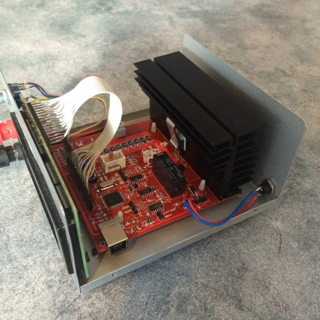
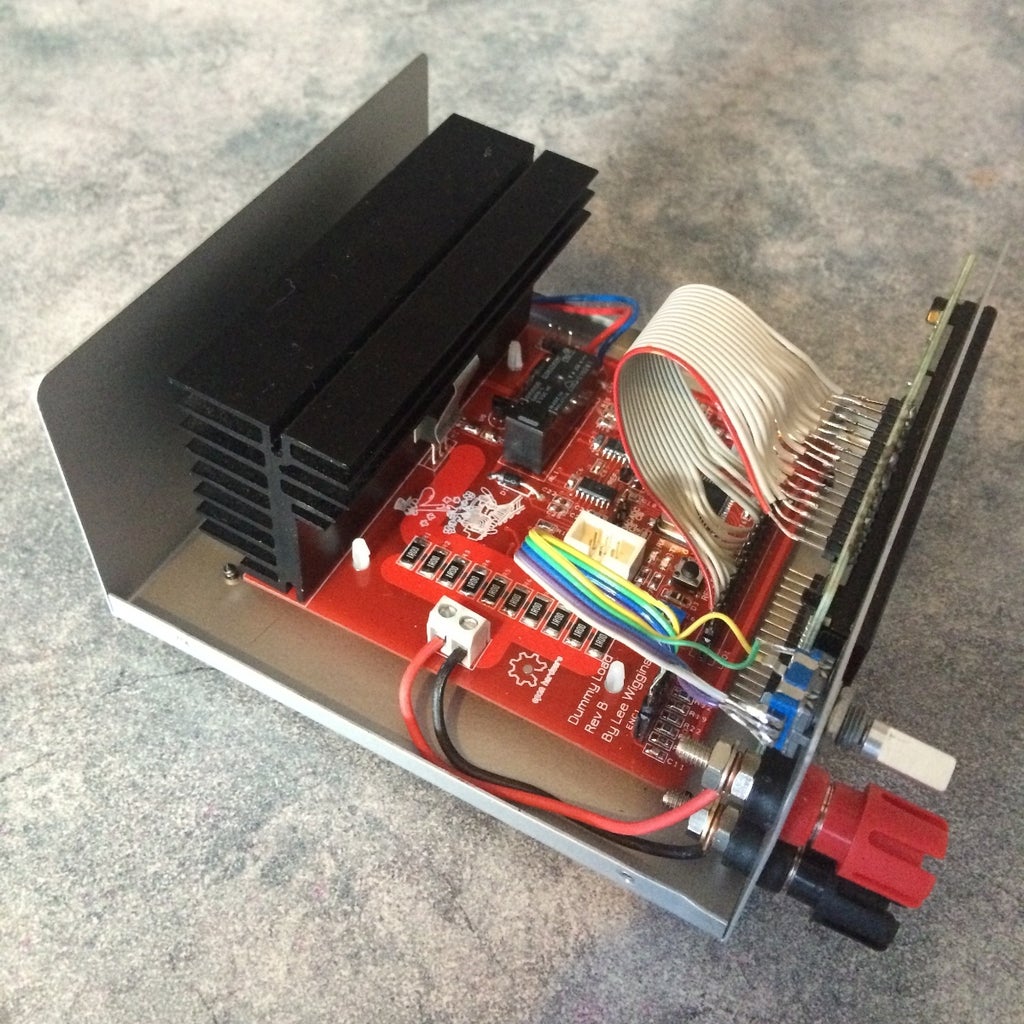
Step 15: The Construction


This was fun!
I ended up mounting it in an aluminium case from Jaycar - HB5444 and mounting it in that as it can get quite hot. I haven't actually mounted the fan properly yet but when I do I will update the photos.
This was my first real PCB layout and yep.. made some errors, all I can say IS CHECK FOOTPRINTS! my ATmega32u4 footprint was an atmel one so I thought.. It will be OK... I was WRONG! the pin spacing was 1mm instead of 0.8mm, I made individual bond wires to go to the pad so I could test it.. NOT FUN, but it worked.
As I said, I did the boards and schematics using DesignSpark which I think is a fantastic open source program with no limitations!
The big fat heavy traces are the load traces they are that big so they can carry the required current, also, that much current can cause quite a lot of noise in the circuit so I put all of the noise sensitive equipment away from it all.
I have boards available on Tindie for $10 each if you're interested. These boards are selling like hot cakes and they are much easier to manage through tindie!
Dave Jones from the EEVBlog kindly did a review of my PCB design for me, watch it below. It starts at 19 minutes 27 seconds
I had the PCBs manufactured by iTead Studio which are a reasonably good quality good value PCB manufacturer. I have included the Gerder files should you want to copy my board on my GitHub, make sure to use rev 2!
Step 16: A Big THANK YOU

Thanks for spending the time to read this instructable, I hope you have found in useful and interesting.
Please leave your comments below to let me know what you thought, my next project is an 8 x 8 x 8 RBG LED cube so I will do an intructable on that also if you have found this one helpful!
Thanks again!
Lee


