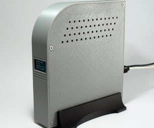
Introduction: Bop It With FPGA Board
Welcome to the Bop It with FPGA Board Instructable,
Project dedicated for CPE 133 at Cal Poly, San Luis Obispo. This project was created by Ian Nielsen and Omri Nissan. Outside codes were involved in various locations and are cited in the Final Project Report File. Questions and suggestions are welcomed via email.
Contact info:
Ian Nielsen: ineilsen@calpoly.edu
Omri Nissan: onissan@calpoly.edu
There is step by step procedures in order to generate this project. All necessary programing files needed to build your own programmable Bop It are attached to this page. If you choose to use our information, please cite accordingly. It is free, but will appreciate recognition.
Thank you for your time.
Step 1: Introduction:
The project you are about to embark on is very unique. Have you ever played BOP IT? Because that is what you will be making.
This sensational electronic game can be produced using a your own FPGA board and enhanced with some simple electrical components. This is a really cool project that involves some time and some work. You have the option to create the different Bot It button motions (bop it, twist, lever, etc.). You can either use the on board buttons to represent the different motions, however the game becomes more like a Whack a Mole. Ian personally made the different motions out of lego. Making those different functionalities is interesting and very unique. If this FPGA Bop It is built right, it can be very fun to play. Most components attached to the main file are very useful programs that can be used to any project beside this FPGA Bop It. For us, this project was very interesting and challenging, we wish we had a bit more time as we were very close to finishing it. It taught us a lot about clock integration in finite state machines and different modules. Overall, it was very enjoyable and exciting project.
The our end result of our FPGA Bop It can be seen on the front page of our Instructable.
Creating our FPGA Bop It according to the original rules of a Bop It raised some issues:
1. Voice integration. It was hard to incorporate voice in the time frame we had. So instead we used on board LEDs to display which button to press.
2. Display LEDs. Lighting LED once in a cycle/wait time. It came into complicated calculations to set the LED on high once in the cycle.
3. Clocks integration. Clocks have become very complex matter as assigning/figuring the right clock for a certain module became confusing. Each module had to run on some kind of clock.
4. External buttons. Getting the buttons to be compatible with the FPGA takes time, especially because we were not prepared for mislabel and other specifications.
We came really close to making our FPGA Bop It work, however those issues have caused the FPGA board to behave not according to our expectations.
Here are some recommendation/improvements if you plan on pursuing this project:
⬧ Review the finite state machine for improvement.
⬧ Review Clk division programs.
⬧ Label your wires.
⬧ See if you are using high to low or low to high connectors.
⬧ Start early, this project is very time taxing.
Step 2: Materials/ Software:
Software:
- Xilinx Webpack 14.5
(http://www.xilinx.com/support/download/index.html/content/xilinx/en/downloadNav/design-tools.html)
- Digilent Adept
(http://www.digilentinc.com/Products/Detail.cfm?Prod=ADEPT2)
Material for external buttons:
- 3 Resistors (200 Ω)
- 3 SPDT switch without roller
- Breadboard
- Wire Electric
- Tape
Step 3: Overall Design:
Top design looks like the image above:
This is displaying the bopit.vhd file. It is the mainframe for the entire program. Every program that we will be talking about is connected to this file. Also the finite state machine resides in this file.
Step 4: Button Setup:
Setting up the buttons simply came down to connecting leads from the voltage source of one board’s 6-pin connector to the desired I/O ports. We ran into a few issues with rigging the setup, so we’d recommend using the Nexys board’s onboard buttons.
Step 5: Finite State Machine:
We wanted our games FSM to be as simple as possible, so we designed it to have three states. The initial state, called idle, simply idles until the user uses the start button to begin the game, setting an enable signal to high. Once pressed the next state is Wait Time, waiting till the end of the current four beats, then the next state is a wait-for-results state where the beat and indicated led are shown. In this state, the machine waits for a result from the comparator that checks the button inputs against the randomly chosen button value. If time runs out without input, the game resets to idle and enable returns to low - this also occurs if the comparator returns not match. But if the comparator returns match, then the next state is wait-for-time-left, in which the machine checks the time over value sent from the timer. Then only from this waiting state, the score is incremented, and the machine returns to wait for input with a new indicated button value.
In retrospect, we could have used two separate FSM’s to individually handle game status (game over or still playing?) and input status (has a button been pressed? Does it match? Is there still time left?).
Step 6: VHDL Modules Descriptions
Timer Counter:
Timer depends on few variables. The main variable is the en, which has been talked about in the finite state machine. This program is the program that makes sure that after certain amount of cycle (in our case 4), the program terminates. If the en =1, then the module adds one to a 3 bit binary number, which is initially at zero, on the rising of clk. Otherwise the counter is reset to zero. There is also an output to display if the time is over or whether you have pressed the right button.
Score Counter:
Functionally, the Counter adds up 1 to the total score if it receives a match signal. Otherwise it the score is set to the previous score. The score is initially set to zero. The score is to resets to zero in the idle state of the finite state machine.
Comparator:
The comparator takes in two 3 bit buses and compares those to busses when the en is 1. On of the buses represents the btns and the other is the LEDs. This comparator is basically checking if the btns and the LEDs match. If they do, it sends a match signal, otherwise the not match signal is being send. If the comparator sees that the btn have not been press, it will not be giving match or not match any signal.
sseg_dec:
Code has been created by Bryan Mealy. This code has few components in it. It converts binary to decimal, manages the seven segment displays with the input value, and it also contain a clock divider.
Clock Division:
The Clock divider code has been written by Bryan Mealy. A clock divider slows down or increases the frequency of the clock. We tweaked the max values to match the time frame/ cycle we were looking for. Our modified clock divider runs on a quarter a second period.
Decoders:
We have only one decoder that assigns the random 8 bit value to different 3 bit values. The 8 bit number represents the random value we are getting from the random bit generator that we will be talked more about in details later. The 3 bit number represents the LED that will be lighting up.
Led Driver:
This module was meant to be the driver for the button and tempo indicator LED’s. The tempo LED simply copied the slowed clock signal from our clock divider, and flashed to the beat of the game. The button indicator LED flashes on for the first two of the four beats shown by the tempo indicator, as it copied the signal of our super slow clock (period of four beats).
Random Button Chooser:
The random button chooser that we had used a pseudo random bit generator, created by a linear feedback shift register (Or LFSR for short). This LFSR is simply a chain of d-flip flops with a few select flip-flop outputs leading into XOR gates that lead back to the first d-flip flop. This chain creates a semi-random sequence that will repeat itself at some point (but not that quickly). This LFSR creates a random eight bit binary number (in decimal, somewhere between 0 and 255), which we then send to our decoder to choose a button. (Our PRBG was modeled after Debashish Mohapatra’s 16-bit PRBG, which can be found herehttp://www.debashish.info/index.php/e-learning/vlsi-design/vhdl-codes/174-prbs-pseudo-random-binary-sequence-generator-vhdl-code-and-vhdl-testbench-creation)
Step 7: Extra Informations/ Recognition:
This project was made by Ian Nielsen and Omri Nissan for a CPE-133 class in Cal Poly. The sseg_dec and the clock divider are made by Bryan Mealy. Any code written exclusively by either Ian Nielsen or Omri Nissan on this Instructable is free to use. If you have any suggestions, questions, or issues with our page, feel free to shoot us emails.


