Introduction: How to Make a Professional Printed Circuit Board: the Complete Guide
Hello everybody, today I will show you how to make professional PCB, to improve your electronic projects.
Let's start !
Step 1: What You Need to Buy
Tin solution (optional but recommended)
NaOH (sodium hydroxide)
Acetone (you can find it in a supermarket)
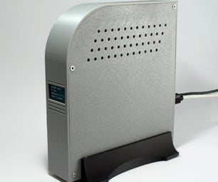
( Here is the link to the project related to the PCB you will see in this tutorial : Computer Control Box )
Step 2: Drawing the PCB
If you already have the design of your PCB in a file, you can skip this step
I am using Proteus software to draw my PCBs, but you can also use Fritzing software to do that. The most important is that you can export your design into a .pdf file. PDF keeps real size so if you print this file to a 1:1 scale, you will not have scale troubles after printing.
Step 3: Printing the Artwork
Now print the PCB design on transparent sheets
I advise you to print a least 3 copies of the artwork, you will get better results because the opacity will be better at the exposing step...
Step 4: Setting Up Chemicals
During these steps, wear gloves and work in a well ventilated area and wear a pair of goggles. You will handle strong bases and acids. Some of them evaporate easily in the air. I also advise you to wear a lab coat or old clothes because an iron chloride spot can not be cleaned. It lets a disgusting yellow-brown color ...
/!\ Never pour liquids containing metals into the environment /! \ Use a bottle of chemical waste that you can give to a waste disposal site.
Prepare a bath of relelator for prepositive sensibilized epoxy. It is just sodium hydroxyde ( concentration 15g/L ) Let it to the room temperature.
Prepare an other bath with a solution of iron III chloride (FeCl3)
If you want the reaction to go faster, you will need to catalyse the reaction between the acid (FeCl3) and copper of the PCB, it means you will need to heat the iron III chloride solution. To do that, I use a hot water bath (see pictures) Without this, the result will not be as expected.
Heat the water in a boiler to a temperature of about 80 ° C, once it is hot pour the water into a larger container than the FeCl3 one. Place the FeCl3 bath in the hot water bath.
Also prepare a water bath, (distilled water is better) to wash the PCB between each steps. It is also a good idea to keep absorbing paper next to you... When you wash the PCB, absorbe water on it to not dilute the next bath.
Step 5: Exposing the PCB
Let's set up the UV-light exposure box.
Take the first artwork and attach it to the pane with adhesive tape. (Be careful about the orientation of the artwork !)
Then add the second and the third design onto the first one to improve the opacity. This trick will prevent UV rays to cross black lines of the design.
Now you are ready. You will work with photosensitive resin, so you will have to work in a place where the brightness is reduced until the PCB is not developed.
Ready to start ? Go!
Carefully remove the protective film of the PCB. Place the sensitive side into the design and secure it in place with tape. Put all of this into the exposure box, sensitive side facing the UV tubes and close the box.
Turn it on between 2' to 2'30" no more. During this, put gloves and goggles to protect yourself from chemicals. Once time is over, switch off the exposure box, open it and take the PCB.
Step 6: Developing the PCB
Place it immediately into the sodium hydroxide bath, sensitive face up. You should immediately see a blue-purple color (sometimes grey) going into the sodium hydroxide. Slowly shake the bath until you great see the design. (Around 30" - 60")
Wash the PCB into the water bath.
Step 7: Engraving the PCB
At this step, the PCB is not photosensitive at all, you can switch on the light !
Now place the PCB copper-face up into the acid bath (FeCl3) and slowly shake it back and forward. The solution always need to move to the reaction take place. (About 20' to 40' depending on the water bath temperature, the surface area of copper to disolve and the concentration of the FeCl3 solution.)
When all copper have been dissolved by the acid, remove the PCB and wash it into an other water bath and dry it out.
Step 8: Washing the PCB
Now you need to remove the remaining resin on the circuit. To do that, place the PBC into an acetone bath. Acetone will become purple. (Around 10" - 20") The copper is henceforth exposed.
Then wash the PCB into water, and you are done !
Step 9: Tinning the PCB
It's an optional step but I advertise you to do it because it will help you to solder components and prevent corrosion.
Place the PCB in a empty bath and pour a little bit of tin II chloride solution on it. It will lay down tin on the circuit.
*** Success ! *** You made a professional PCB !
Step 10: Drilling the PCB
Use a vertical drill and a 0.8mm drill bit to drill every holes, and if the pin of the component is too large to go through, use a 1.2mm drill bit to enlarge the first hole. ( Always start with the smaller drill bit you have, to drill a precise hole ! It is very important ! )
And your PCB is done ! The only remaining thing is to solder your components on it !
I hope you like this tutorial
If you have any question, leave a comment ! ;)
( Here is the link to the project related to the PCB you saw in this tutorial : Computer Control Box )


