

Introduction: How to Make PCB at Home


Website Link : www.link.blogtheorem.com
Hello everyone,
This is instructable is about "How to make PCB at Home" without any special material.As a Electronics Engineering student, I try making DIY projects which require simple electronics circuit and making PCBs.
What is PCB?
A printed circuit board (PCB) mechanically supports and electrically connects electronic components using conductive tracks, pads and other features etched from copper sheets laminated onto a non-conductive substrate.
A printed circuit board has pre-designed copper tracks on a conducting sheet. The pre-defined tracks reduce the wiring thereby reducing the faults arising due to lose connections. One needs to simply place the components on the PCB and solder them.
Different method to make PCB
There are in all three basic methods to make PCB
1. Iron on Glossy paper method
2. Circuit by hand on PCB
3. Laser cutting edge etching.
Since laser method is industrial method to make PCB we will get in detail of first two method to make PCB at home.
Step 1: Creating PCB Layout of Your Circuit
This is usually done by converting your circuit's schematic diagram into a PCB layout using PCB layout software.There are many open source software packages for PCB layout creation and design.
Some are listed here to give you a head-start:
2. PCBWizard
I designed my circuit schematic in Cadsoft Eagle.
Note :In Eagle: File> Export>Image Be sure to set DPIG to 1200 for better quality
Step 2: Material Required

You need also: Permanent black marker, blade cutter, sandpaper, kitchen paper, cotton wool, some old clothes.
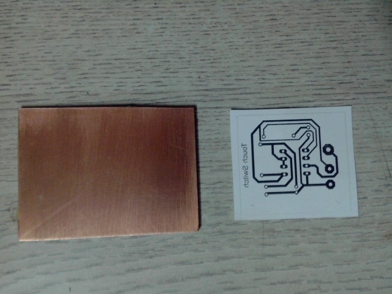
To start making PCB, consider a simple project TOUCH SWITCH using IC555
Step 3: Take Printout of PCB Layout

Take a print out of your PCB layout using the laser printer and the A4 photo paper/glossy paper. Keep in mind the following points:
- You should take the mirror print out
- Select the output in black both from the PCB design software and printer driver settings
- Make sure that the printout is made on the glossy side of the paper
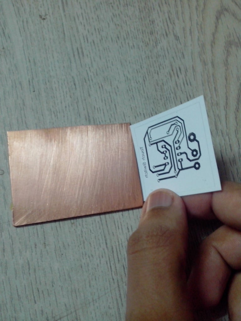
Step 4: Cutting the Copper Plate


Cut the copper board according to the size of layout.
Step 5: Make It Smooth

Rub the copper side of PCB using steel wool or abrasive spongy scrubs. This removes the top oxide layer of copper as well as the photo resists layer.
Sanded surface allow image to stick better
Step 6: Methods

Method 1:
Iron on Glossy paper method: Transfer the printed image from the photo paper to the board. Make sure to flip top layer horizontally. Put the copper surface of the board on the printed layout. Ensure that the board is aligned correctly along the borders of the printed layout. Put tape along the two sides of the board non-copper side. This will help to hold the board and the printed layout in position.
Method 2:
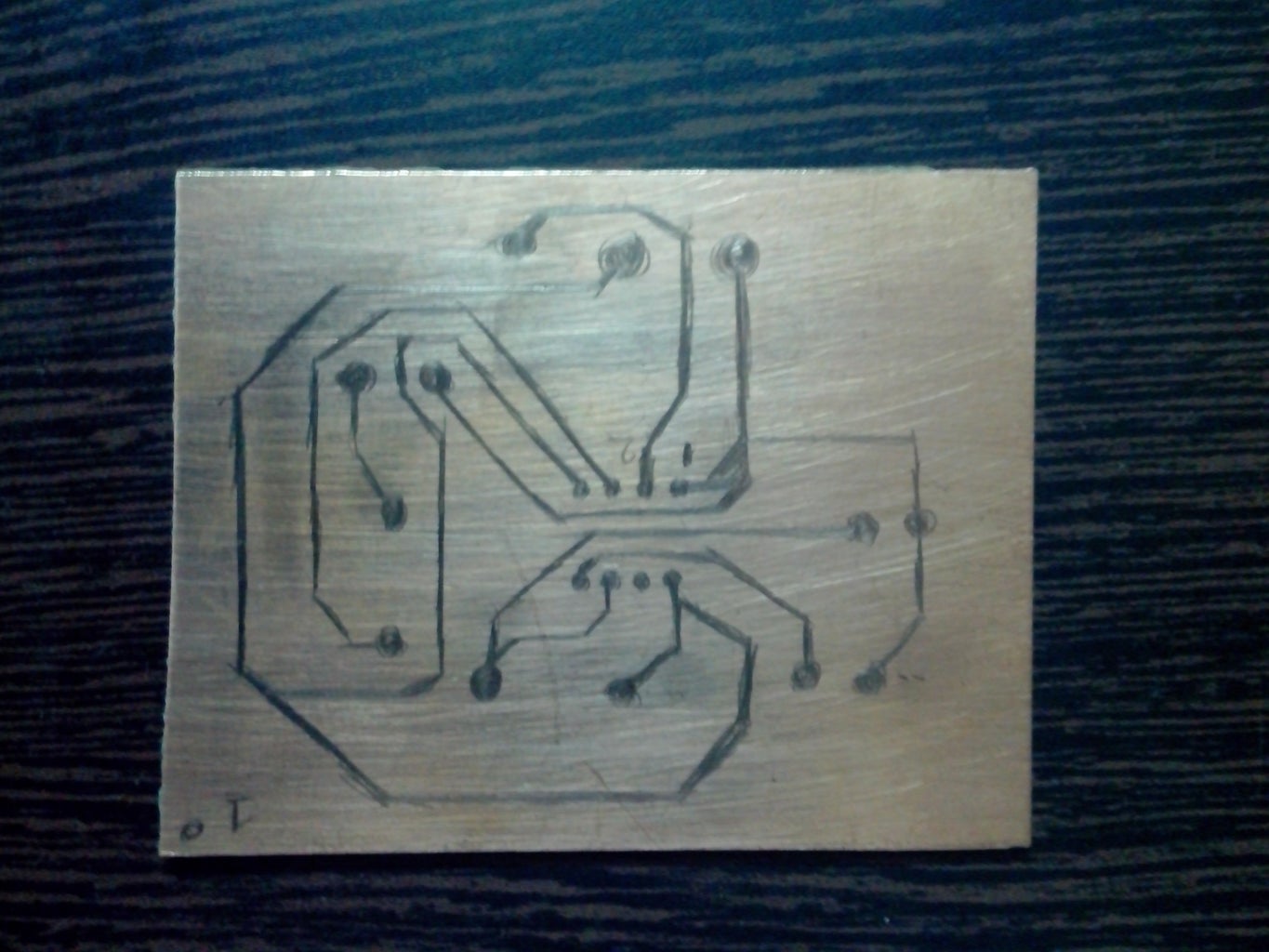
Circuit by using permanent marker: Using reference of circuit image printed on glossy paper first draw basic sketch on copper plate with pencil and then by permanent black marker.
Step 7: Iron It!


- After printing on glossy paper we iron it image side down to copper side. Heat up the Electric iron to the maximum temperature.
- Put the board and photo paper arrangement on a clean wooden table and clothes with the back of the photo paper facing you.
- Hold one end of it by the Towel and put the hot iron on the other end for about 10 seconds. Now, iron the photo paper all along using the tip and applying little pressure for about 5 to 15 mins.
- Pay attention towards the edges of the board – you need to apply pressure, do the ironing slowly.
- Long hard press seems to work better than moving iron around.
- Here iron heat melts ink printed on glossy paper and get transfer to copper plate.
CAUTION: Do not directly touch copper plate because it is very hot due to ironing.
Step 8: Peeling


After ironing, place printed plate in Luke warm water for around 10 minutes. Paper will dissolve and remove paper gently. Remove the Paper off at low angle & traces.
In some cases while removing paper some of track get fainted .
See figure in white box black line track is light in colour hence we can use black marker to dark lighted track as shown in image
Step 9: Etching


You need to be EXTREMELY careful & cautious while performing this step
• First put rubber or plastic gloves.
• Place some newspaper so that etching solution do not spoil floor.
1)Take a plastic box and fill it up with some water.
2) Dissolve 2-3 tea spoon of ferric chloride power in the water.
3) Dip the PCB into the Etching solution (Ferric chloride solution, Fecl3) for approximately 30 mins.
4) The Fecl3 reacts with the unmasked copper and removes the unwanted copper from the PCB.
5) This process is called as Etching. Use pliers to take out the PCB and check if the entire unmasked area has been etched or not. In case it is not etched leave it for some more time in the solution.
Gently move plastic box to and fro so that etching solution react with exposed copper and form iron and copper chloride.
After every 2-3 minutes check whether all copper is etched or not.
Step 10: Caution

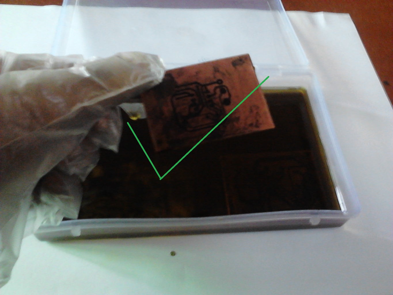


DO NOT DIRECTLY TOUCH ETCHING SOLUTION USE GLOVES
In figure we can see that copper is slowly getting etched.
Step 11: Disposal
The etching solution is toxic to fish and other water organisms.
Don't pour it in the sink when you are done. It is illegal to do so and might damage your pipes.
Dilute etching solution and then dispose the solution.
Step 12: Final Touch
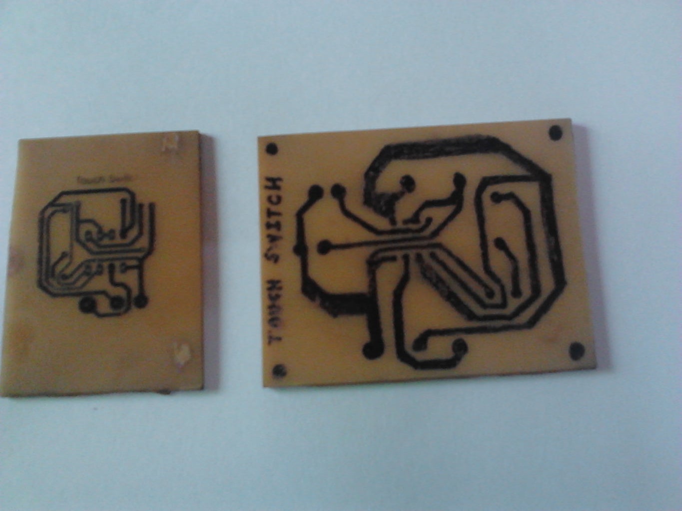


Figure show PCB of both circuit made using print out and using marker.
A few drops of thinner (nail polish remover works well) on a pinch of cotton wool will remove completely the toner, bringing back the copper surface.Rinse carefully and dry with a clean cloth or kitchen paper.Trim to final size and refine edges with sandpaper.Acetone help glossy paper stick to rough paper.
Drill hole and solder all the component & PCB is ready. Cheer!!
Step 13: Conclusion
1. Iron on Glossy paper method is efficient method to make pcb at home. If done carefully each track can be perfectly printed.
2. Circuit by hand on PCB is limited to our artistic skills. Simple circuit can easily be made by this method but for complex pcb Iron on Glossy paper is best.
Step 14: More at BlogTheorem.com

Thank you are reaching till this point of instructable. I will take just few seconds.
You can visit my website - www.blogtheorem.com where I made interesting article on Science,Engineering & Technology related.
Top 4 Best Free ML course | 2020 | Online | Projects

Participated in the
On a Budget Contest

Participated in the
Burn It! Contest

Participated in the
Explore Science Contest


