Introduction: Op-amp Headphone Amplifier
This is a headphone amplifier similiar to the one designed by Chu Moy. For reference, the original Chu Moy article is here while a great tutorial on building it is here. I have used a different dual operational amplifier, the RC4560, manufactured by Texas Instruments, in the TSSOP package, and chip resistors in order to make an extremely small printed circuit board assembly.
Step 1: The Op Amp
The active device is the RC4560, which Texas Instruments claim to be suitable for, among others, Headphone amplifiers. It can work down to +/- 2 volts, and has low noise and a wide enough bandwidth.
It is available in a TSSOP (Thin Shrink Small Outline Package) which means it is small indeed, small enough for me to demonstrate my one-off microprototyping skills.
Step 2: The Circuit
The circuit is the standard non-inverting amplifier with a gain of 11, with a capacitively coupled input. A small valued resistor at the output of the amplifier isolates the load and minimises any tendency of oscillation with long headphone leads.
The large size of the input capacitors make them too bulky to be included on board, so they shall be outside, between the input jack and volume control, and the board.
The power supply is provided by a nine volt battery, converted to dual +/- 4.5 volts by 4.7K resistors and decoupled by 220 microfarad capacitors.
A high efficiency Light Emitting Diode shall provide indication that the circuit is ON, it is fed with about 0.7 milliamperes by a 10K resistor.
Step 3: The Components
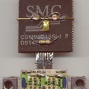
The picture shows the integrated circuit and resistors. The chip is a free sample from Texas Instruments, and the resistors are all scrounged from old hard drives. The four digit marking means they are all of 1% tolerance, and they might even be MFR (metal film resistor). There is absolutely no way to confirm this, however.
The small size of these components make it very difficult for conventional point to point wiring techniques to be used. In fact the only viable means of connecting them up is to use a printed circuit board.
Step 4: The Printed Circuit Board - Design
Before etching the PCB, we need a design. Since there are a total of nine components on board I opted to use the simplest, most widely available CAD tool for this purpose - the Windows Paint.
In the design below, black represents copper, white repesents the areas where copper has to be removed, and grey and yellow represent the component body and leads respectively.
The component outlines can be removed, the gaps cleaned up, and the pattern printed to scale using a laser printer, mirror imaged of course, and the pattern ironed on to copper laminated board, and etched in ferric chloride.
Since I was going to make a grand total of ONE board I opted for a different approach. (I could not find the chip resistors for a second board.) And that was to draw the pattern directly onto the laminate using a permanent marker.
More specifically, I coated the laminate (after cleaning) with a coat of etch resist (permanent marker ink) and scratched the pattern on to it with a sharp point.
Step 5: Preparing the Board
I used the salt water etch process, documented here in instructables to make the board.
A small piece of double sided copper clad epoxy board was cut to size and cleaned. Reference marks were punched on it so that when covered with a layer of marker ink these will still be visible. The lines and punch marks do not cut the copper, they just indent the surface just enough to mark it in relief.
Step 6: Coat With Resist
The other side of the board was covered with a layer of duck tape. This side is covered with a layer of permanent marker. The markings are still visible.
Step 7: Scratch Pattern
The places where copper is to be removed was scratched to expose the underlying copper using an awl.
If you have a dremel with a pointed tool, a steady hand, and lots of confidence (or lots of board) you can skip a few steps and carve the board directly. This saves the bother of messing about with chemicals in order to remove the copper.
But doing it this roundabout way has advantages: mistakes can be rectified by dabbing on a spot of marker and scratching again. Designing those lines to be straight was easy in Paint, and while drawing it on to the board, a transparent ruler can be used to guide the awl through those lines.
When all mistakes have been rectified and the board looks like the intended design solder a wire to the copper, drop it in some salt water and make it the anode for five minutes or so.
Step 8: The Etched Board
This is how the board looks after copper removal by electrolysis, and removing the etch resist by wiping with acetone.
Those lines were scored into the copper as a guide, and copper remains over some parts. You can also see that copper remains in some places near the edge of the board, this is intentional, and is designed so that the current has a path to travel to all parts of the board so that electrolysis can proceed.
Some bridges remain across those gaps, and will be cleared by running the edge of a sharp knife through them. After testing (using 12W lamp and battery) and a coating of varnish it is ready for soldering.
Step 9: Resistors Soldered
The resistors have been soldered into position, together with some links to the other side - the + 4.5 V and - 4.5 V supplies to the op amp, and the ground to the junction of the 100K and 1K resistors are made with wires inserted into holes drilled with a 0.7 mm bit, and soldered on both sides.
Step 10: Soldering the Chip
The chip has been soldered in. If the measurements of the pattern was correct this should sit with its leads in the middle of the pads. If the pads have been tinned with a bit of solder and given a light coating of flux, placing it in position and applying heat from the pointed tip of the soldering iron will be sufficient to attach all its leads.
I use the tip of a length of copper wire wrapped around the bit of the iron in order to successfully heat one joint without disturbing the one next to it.
Jewellers eyeglass screwed into the eye is good, too. Leaves both hands free to grope around the desktop looking for tools you dropped.
Tip: LOOK for the soldering iron, do not try to locate it by feel.
Step 11: The Other Side of the Board
I used a double sided board, and the intention was to use one side of the board for the signal and the other side for the power related components.
Four links join the top and bottom sides of the board. The other side was prepared for the power supply circuitry by removing the copper to isolate the + and - supply connections to the chip. These cuts were made with the sharp point of a hobby knife.
The picture shows the two 4.7K resistors for the "virtual ground" and two 100n ceramic chip decoupling capacitors. These capacitors are not drawn in on the schematic, but op amp lore has it that it is good to have them. Better drop them in now than later, when there might not be space left on board for them.
Step 12: The Other Components
Now that the board is complete, it is time to look for the other components which shall make up the headphone amplifier.
A 9V battery has been included as a reference for size. The top off a dead 9V battery is used for the battery connector. A broken stereo jack shall be processed into the input connector. A volume control has to be harvested from somewhere. I am still in the field, looking out for one. A bright green LED that gives out a satisfactory amount of light when fed with 10K from that 9V battery has been selected. The two input capacitors are 150 nf (0.15 microfarads) which is 50% more than specified, and so adequate for the purpose. The two electrolytics have voltage ratings of 16 volts, and so they will be okay in this circuit which has a maximum of nine volts.
I am also in the lookout for a container for these bits and pieces. For a demo, a transparent case should do, though a metal case should be used for the sake of shielding.
The output shall be a female stereo receptacle that attaches to the end of a cable. This shall enable the actual box itself to be very small.
Step 13: Reverse Polarity and Overvoltage Protection
Before connecting up that battery snap, I began to think. What if the power source was sometimes connected up in reverse? This would not be probable with a battery, but I might add a jack for a wall wart and then that becomes a likely scenario. And what if the wart delivered too much voltage? And, when to know that the battery was due to be replaced?
Reverse polarity protection may be implemented by a diode reverse connected across the supply leads of the op amp. Then, if a voltage source is connected in reverse, the diode will conduct and hopefully the ic will not be subjected to more than a volt or so of reverse voltage.
Make that diode a zener, and it will conduct when its rated voltage is reached.
I added a zener of 24 volts, so that two 9 V batteries in series can be accommmodated, and still keep within the 36 volts rating of the RC4560. Besides, this diode was there in my junk box.
There was another one of 2 volts in there, and I put that in series with the LED. My additions to Chu Moy's circuit is highlighted below. Now when the LED goes dim or remains off you know that the voltage of the battery is below four volts or so and it is time to swap it out for one with more juice.
Step 14: Power Supply
The figure shows the power supply implemented. The LED (green) needs about 2.5 volts to light up, and the zener in series with it needs about 2 volts to conduct. So the LED will go out when the battery voltage gets lower than 4.5 volts. The zener can be of a higher voltage if an earlier warning of low battery is desired.
The zener for protection is placed on board so that frayed leads etc do not cause the protection to become ineffective.
The two electrolytics forming the virtual earth have been connected with three pieces of wire so that the whole assembly may be packed into a minimum of space.
Step 15: The Signal Connections
The figure shows the connections for the signal. The earphone jack gets plugged into the music source, and the left and right signals get to the amplifier through the two .15 microfarad plastic dielectric capacitors (blue). The brown wire is ground (sleeve). Green is right (ring), and white is left (tip).
The output from the amplifier board feeds a socket to mate with the headphone jack. I have taken one channel direct from the opamp output, and the other from the isolating resistor. After extensive tests the connection with the better sound (I hope) will be selected for both channels.
The on-off switch has been placed on the battery connector. So this picture shows the entire headphone amplifier, as well as the cheap earphones I am using to test it with.
So how does it work?
It doesn't.
Step 16: Troubleshooting
I quickly established that the virtual ground point approached the positive supply rail whenever the earphones were plugged in. The outputs of the amplifiers were sitting at about 100 millivolts positive, and the resulting current through the earphone coils were overpowering the 4.7K/4.7K voltage divider virtual ground.
The RC4560 is a bipolar opamp (price $0.41 each according to the TI website) and so it has an input bias current which can go up to 0.5 microamps according to the datasheet. This current (100 nanoamps in my case) across the input resistor of 100K was developing an input offset of 10 millivolts, which, amplified by the gain of 11, resulted in the offset at the output. The amplifier and its circuit was behaving normally, as all op amps do. It was my expectations regarding the circuit that was wrong.
What could be done? I could purchase two OPA627's (price $12.25 each according to the TI website) and place them in place of that RC4560. Well no. There isn't sufficient space.
The difficulty was that the offset at the output of the opamps was causing a current to flow. What if the current was prevented from flowing? The offset, or any steady voltage at the output, for that matter, was not signal. So I added a small capacitor between the virtual ground and the junction of the two 220 microfarad caps, and allowed the ground return of the earphones to sit at whatever voltage they cared to.
With this modification the circuit worked as a headphone amplifier.
How does it work? (again!)
Well, I do not have decent headphones to check it with, so the only thing I can say with confidence now is that it does sound louder.
Step 17: The Amplifier in Action
This shows my amplifier hooked up to my compact audio disk player. The volume control inside this player has a good range of adjustment at the low end, so I can do without a volume control in my amp for the time being.
And oh yes - my taste in music is atrocious.
Listening to a couple of disks did not bring up any problems that might need attention, so I looked around for a box to put it in. A metal box is to be preferred, but the wiring is so compact that there isn't much enclosed area or stray capacitance to pick up noise, even without the shielding of a metal box.
Having the input jack and output socket at the end of cables mean that the box can be small indeed, if the volume control is not fitted.
For the present, I have stuffed it into a transparent plastic box.
Step 18: Amp in a Box
The amplifier looks neat inside this little plastic box. There is just sufficient space for the battery and the circuit board to fit side by side.
I shall either line this box with metal foil or try and find a metal box this shape and size. The jack and socket shall be connected with the proper cable. An extension stereo cable, one with a plug at one end, and a socket at the other, can be cut and the amplifier introduced in the middle, for a neat solution.
Step 19: All the Bits on One Page
Here I have drawn the circuit diagram of the entire device as one, in order to assist anybody who would like to duplicate this circuit.
This started out as a "Chu Moy" circuit, but now the deviations from that ideal make this a different sort of beast.
The original Chu Moy amp uses FET input opamps. This one uses a far cheaper bipolar one. The virtual ground, at which the headphone common terminal sits, is now floating.
The amplifier was not built on board with oxygen-free copper cladding. Instead of new pedigreed precision resistors those from junked hard disk drives were used.
Be warned. Listening to music that has passed through such plebian devices for an extended period of time can do things to your mind. You will no longer be able to pass a pile of junk without an uncontrollable urge to dive inside it and retrive what you can. And you might even arrange those pieces of junk, call it by some pedigree name, and post the result in some website.
Like me.


