

Introduction: PCB Etching (prototyping)


Making circuits is great but what if you want to make your ideas a bit more permanent? That´s when it´s great to be able to make your own PCBs at home.
I´ll show you how to make your own single sided Printed Circuit Boards at home. If you want to get one step further you can also learn how to tin and apply a solder-resist dryfilm to it.
Step 1: Things You Need.


Chemicals:
- Sodiumpersulfate - Na2S2O8
- Sodium Carbonate aka. washing soda - Na2CO3 (Optional only for dry film)
- Distilled water
- Fotopositive developer - NaOH
Materials:
- Foto coated PCB
- Printer film
Tools:
- Rotary tool
- Jigsaw (only if you plan to cut out something on your pcb)
- Nibbler (can be handy)
- Plastic tweezers
- Something for sanding
- Brush
- Exposure unit with frame* (UV lamp)
Etching unit (or beaker and heatplate)
Others:
- Gloves
- Open container for developing
- Eye protection
- Funnel (for filling liquids back into their bottles)
Optional:
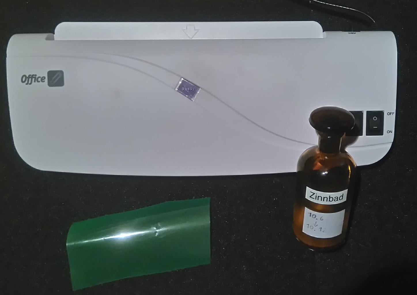
- Dry film solder stop laminate
- Laminator
- Chemical tinning fluid
*I´ll show you later on
Step 2: Create and Print Your Layout.


1. Use your favourite Cad Software (mine is Cadsoft eagle) to design a PCB layout.
2. Open the layer settings and only enable the copper (top or bottom, depending on what type of pcb you´re planning to make), the pads, the Vias and the dimension layers.
3. Put some printable transparency films into your printer.
4. Press the print button in your cad software and print out a black, real-scale version of your layout. Depending on your printer you may have to print the layout twice and then stick the two printed films on top of each other to get a fully light stopping image.
If you want to add a solder resist later on:
1. Get back to your Cad software and open the layers menu
2. Now only enable the top-stop layer (or the bottom-stop layer, again depending on the type of pcb you´re planning to make)
3. Repeat the point 4.
Step 3: Expose the PCB


1. Peel off the protective layer from your PCB. Make sure you don´t touch the copper side of the PCB after removing the protective layer because if you do you´ll have problems developing it
2. Align the printed film and the PCB so that all of the traces on the film have copper underneath them.
3. Put the PCB and the already aligned film betwen two glass plates to keep the film flat on the surface of the PCB. Use some magnets to hold the glass plates together (like shown in the pictures)
4. Now expose the PCB to UV light. I used a 25W party UV light and it took about 5 minutes to finish exposing
Step 4: Developing the PCB


Now it´s time to put on your gloves and eye protection.Don't take them off during the entire etching process
1. Mix the developer following the description on its package. I´ve never tried it myself but 10g of NaOH in 1 litre of water should work as well.
2. Put your PCB into the developer solution immediately after finishing the process of exposing.
3. Use your brush to help the developer remove the photoresist.
4. Do this for about 30 seconds until no photoresist is coming off anymore but don´t take it out yet. Let it develop a little bit longer than it seems to need. That way you can be sure that all of the unnecessary photoresist is removed. Otherwise your etching results will ruin your day.
5. Rinse the PCB with tap water and move on to the next step
NOTES:
- When you have finished developing take your developer and pour it into your sink. It´s basically the same stuff used for drain cleaners.
Step 5: Etching


1. Mix your etchant: Use 250g of sodiumpersulfate (Na2S2O8) per litre of distilled water.
2. Pour the etchant into your etching unit and heat it to 50 °C (don´t overheat it because sodiumpersulfate starts to decompose at over 50°C)
If you don´t have an etching unit just fill the etchant into a heat resistant beaker and put it on top of a heatplate. Also heat it up to about 50°C
3. As soon as the etchant has reached its final temerature take your PCB, put it inside and start the air supply of your etching unit (If you use the beaker method take a stirring rod and just stir the solution with the PCB in it.)
4. Leave it inside the etchant until all of the copper has "disappeared"
5. Rinse the PCB with tap water.
6. If you use an etching unit make sure you take out the etchant and store it in another not airtight container. Otherwise your air bubbler may get damaged.
NOTES:
- The etchant will turn blue and start getting inefficient after a couple of PCBs. When you realise that the etching process starts taking way longer, change your etchant and take the old one to your local chemical waste center Warning: "The used etching solution contains dissolved copper which isn´t good for your environment "
Step 6: Tinning (optional)


1. Remove the excess photoresist by cleaning the PCB with acetone
2. Take your tinning fluid and fill it into an open container.
3. Put your PCB into it and leave it in there for about 5 - 10 minutes
4. Take the PCB out of the solution and rinse it with tap water
5. Pour the tinning fluid back into a glass bottle using the funnel. Store it in a place where no pets or kids can reach it.
NOTES:
The tinning fluid is reusable, but after some time the efficiency will decrease. If this is the case bring it to your local chemical waste center.
Step 7: Drilling

1. Take the rotary tool and the right sized drill bit.
2. If you have a drill stand, fix your rotary tool in it.
3. Make sure you´ve got good light so that you can clearly see where the holes need to be.
4. Drill all the holes you need
5. Clean your pcb.
Step 8: Photoresist (the Next Few Steps Are Optional)


Before you start, turn on your laminator so you don´t have to wait for it at point 6.
1. Get some Solder resist dry-film
2. Then dim the lights and take it out of its lightproof packaging
3. Take two pieces of strong tape and stick them to the top and the bottom side of one corner.
4. Then pull the two pieces of tape apart like shown in the pictures. You´ll end up with one transparent and one green layer. Put the transparent layer to the trash and hold on to the green one.
5. The green layer has got two sides, one side is mat and the other side is shiny. Take your PCB and lay the mat side of the dryfilm onto it. Make sure you don´t get any bubbles in between them.
6. Once your laminator has reached its final temperature (which should be about 150 °C), put your PCB onto a piece of paper and run it through the laminator 2 - 5 times. Just make sure that the entire PCB gets hot.
Step 9: Exopse the Laminate


1. Take the film for the solder mask you printed in step 2 and align it with your PCB.
2. Again clamp the PCB and film between two glass plates using some strong magnets.
3. Expose the PCB to UV light (It takes about 6 minutes with my 25W UV lamp).
4. Now you have to let the PCB rest in a dark place for about 1 hour.
Note: All the areas that don´t get exposed to the UV light will come off in the development process.
Step 10: Developing the Dryfilm


1. Mix the developer by dissolving 10 g of sodium carbonate into one litre of water (You won´t need the whole litre. I just used 100 ml of it)
2. Remove the last transparent protective layer with the help of some adhesive tape (like shown in the pictures)
3. Put your PCB into the developer solution and use a brush to help the developer remove the solder resist from all of the pads.
4. When all of the unnecessary dryfilm has been removed take the PCB out of the solution and rinse it with tap water.
Step 11: Hardening the Dryfilm

1. Take your PCB and harden the dry film by exposing it to UV light. With my 25 W uv lamp it takes about one hour (I expose it for 1/2 hour then I let it cool off and after that I expose it for another 1/2 hour)
2. You can make sure that it has finished hardening by trying to scratch the dryfilm with your fingernail, you shouldn´t be able to scratch it after hardening.
Step 12: Cut Out Your PCB

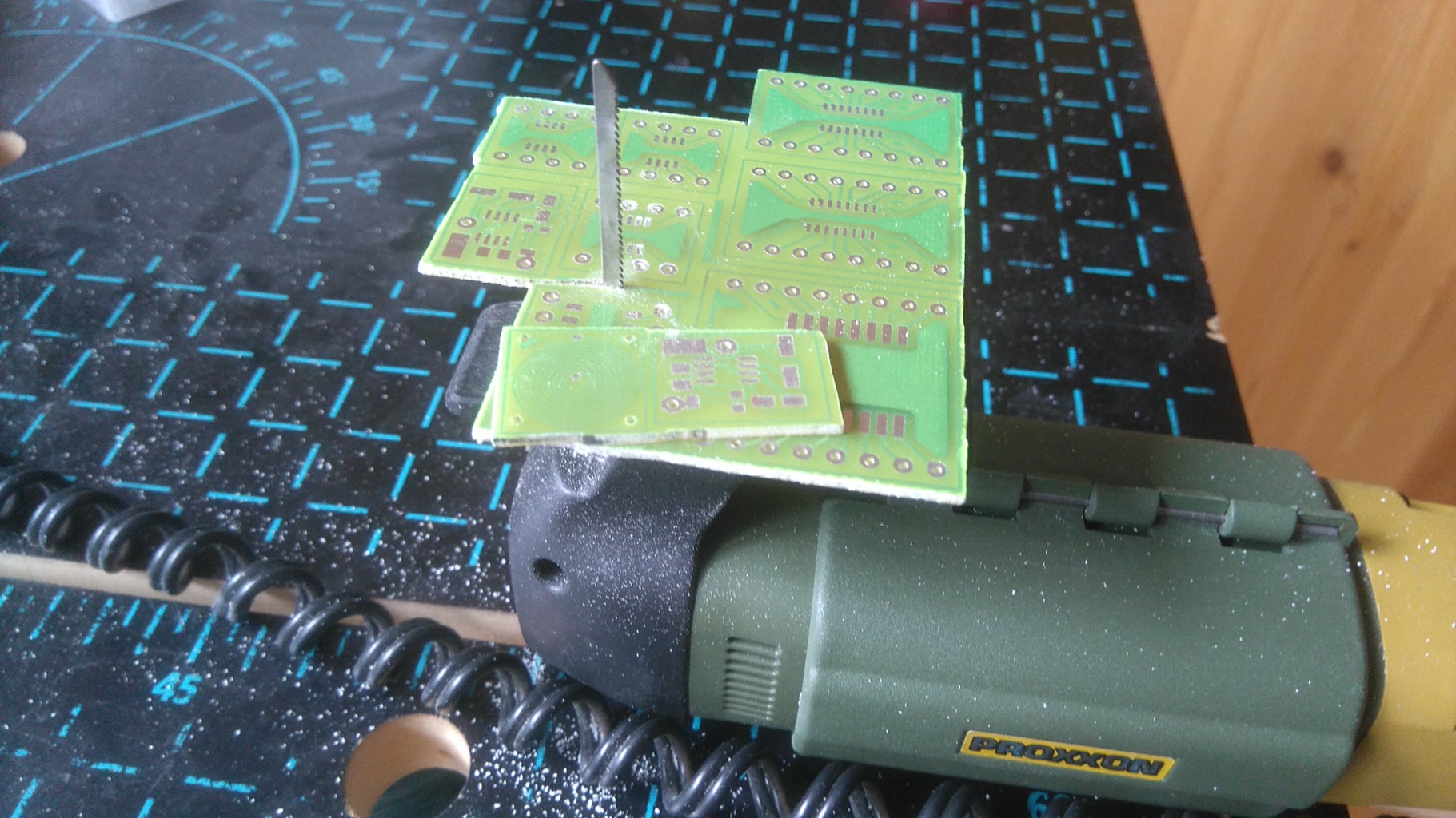

If you´ve done it like me you will now have to cut out your tiny boards, if not you´ll just need to cut the outlines of one board.
1.(optional) Use a nibbling tool to cut out the rough shape of your PCB
2. Use a jigsaw to follow the outline of your PCB(s)
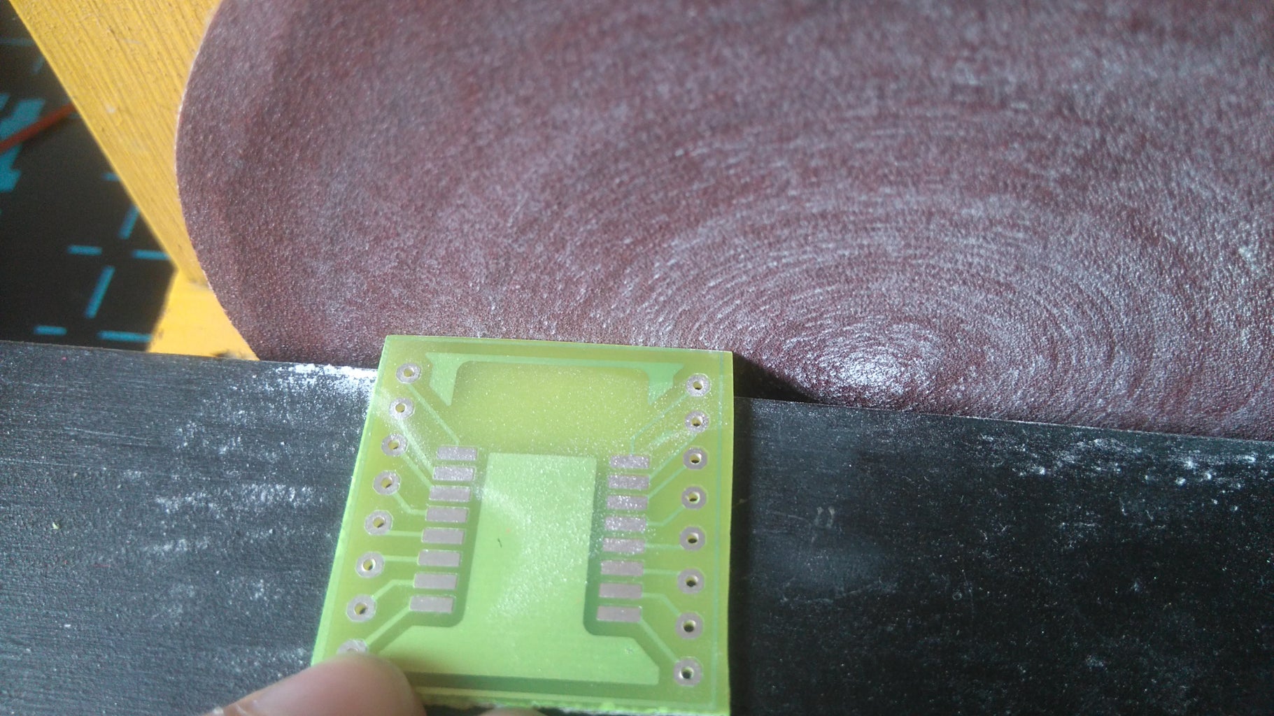
3. Use a sanding block, a file or a discsander to give your board(s) a nice finish.
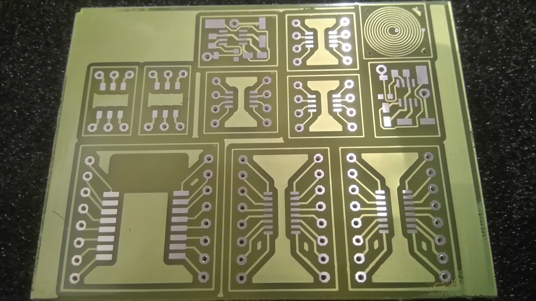
Step 13: Now You Have Your Very Own Printed - Circuit - Boards


You are done!
That´s how simple it is to make custom printed circuit boards at home.
As you can see in the pictures the quality is quite nice. There are some tiny imperfections which are caused by the resolution of my inkjet printer.
Thanks for your attention!
I hope you like this Instructables. If you have any questions share them in the comments and I will answer them as soon as possible.
If you make a PCB with the help of this instructables post a picture in the comments - I´d love to see your results.
Stay safe !
Participated in the
Circuits Contest 2016


