

Introduction: Small Form Factor DIY Arduino on Stripboard


It is not Arduino compatible in the meaning of taking shields (just like every small form factor board isn't).
But it has all the same pins (exept 3.3V power and Vin*) available as female headers. The input and output pins that are right next to each other on original Arduino, almost are the same here, except digital 4 and 5. That means the order is:
RESET	0	1	2	3	4	VCC	GND	_	_	5	6	7	8
9	10	11	12	13	VCC	AREF	GND	A0	A1	A2	A3	A4	A5
It has power indication LED. Not an essential part, but it reminds you to remove the battery when not in use and I have also found it to be useful to notice shorts in my circuit – the power LED goes dim in that case.
It does not have 13th pin LED.
* - Mine has only 9V battery clip directly soldered to it, but this is the easiest part to modify. It also does not have ICSP header, but in the rare case a ISP programmer would be needed it is possible to access all these pins through female headers or remove the Atmega from socket.
So what's the purpose of such thing? I felt I needed a secondary controller besides my usual Arduino for testing things out. I missed that when programming my robot for a contest where IR transmitters were supposed to indicate important places and my attempt to make ATtinys do similar transmission failed. And now I have a task of learning about radio modules ahead of me and I want a familiar platform to test them out before trying to also mess with microcontrollers new to me that are supposed to go into the final product.
When considering the price remember these aspects:
- Do you already have FTDI cable or for how much can you purchase it? (I managed to make one myself, but it takes precise etching and SMD soldering. Also the needed chip is not super cheap for experimentation. Further details https://www.instructables.com/id/FTDI-cable/ )
- Do you have an Arduino (in working order) or AVR programmer to use for burning bootloader on a blank ATmega or can you get the controller with bootloader for reasonable price?
If all that described suits you and you feel ready to do some tightly packed soldering – it really wasn't too easy to get all wires to their right spot – then here is my documentation of the project.
Step 1: Gather Stuff

Medium level of experience in soldering – this is really tight packed project and it's going to be really hard to fix cold or too messy joints in there.
Some understanding of electronics circuits and schematics preferred. You should be able to check the connections, firstly because it is really easy to make some mistakes in a circuit of this complexity level and secondly because I made the final drawing only after finishing my job and fixing couple of mistakes in it which means actually no one has yet made it „following the schematic“ and I might have passed a mistake in even though I did my best not to. Let me know if you find anything suspicious.
Materials:
- ATmega328 or 168. With bootloader (or a working Arduino or AVR programmer to use for burning it)
- Stripboard – piece of 11 x 22 holes where strips run parallel to the shorter edge, but see note about the button type.
- 7805 voltage regulator
- 16MHz crystal oscillator
- Pushbutton („mouse type“) – used as reset button, see images what the „mouse type“ means. You could use the regular round pushbutton in square housing, but it's footprint is wider and then you must make the stripboard wider by one or even two holes. Mouse button saves room here. If you have a broken mouse form recent decade, they actually can be found in there usually.
- 28 pin socket for the ATmega
- Female headers - 2 x 14 or 14 + 8 + 4
- Male headers – 6 pc. For FTDI cable connector.
- 2 x 22pF capacitors (ceramic) – for the crystal
- 4 x 10nF capacitors (ceramic)
- 100nF capacitor (ceramic)
- 100uF electrolytic capacitor (rated 16V or more)
- 1 Kohm resistor – for reset pullup, 1/8 W is best size for my perfoboard schematic.
- ~330 ohm resistor – for the power indicator LED, can be other resistance value suitable for the LED, should be ¼ W, because there will be some power dissipation.
- Rectifier diode – to protect against accidental reverse voltage. These can be found in all kinds of old power supplies – computer PSU, phone charger etc.
- 9V battery clip – can be made form old 9V battery, but be careful while disassembling the metal outer part, I always manage to hurt myself in that process.
- Wires – any insulated wire thin enough to fit through stripboard holes.
- Paper and glue or sticker paper – for pin labels
- Duct tape, double sided tape, cardboard – for protecting the bottom side
Tools:
- Soldering iron and all the rest usual tools needed for soldering job.
- Some means to cut the stripboard in shape (tin shears for laminated board, a sharp knife and wooden block for breaking a plastic one)
- Mini drill with some small grinder bit or other preferred means for cutting and removing traces on stripboard. On my drawing I marked entire surrounding of a hole to be removed, if you make just thin cuts, then in some places they should go in between holes instead of on the hole – especially I mean the male header pins area.
- Multimeter for troubleshooting.
- Components for testing some sketch (for blink sketch led and resistor for example).
Other:
- FTDI cable. But if you are just going to order one and want to make this thing before it arrives you can actually test it out with help of an Arduino that has controller chip in a socket - check out further information in last steps.
Step 2: Schematics


1. The drawing by hand is the clearest schematic I could come up with. I suggest print it out and fold together so that the top and bottom schematic match, it makes it easier for the brain :)
On the bottom the grey squares mark where trace on the stripboard should be removed. On top there are all components marked as symbols or footprint or both. I made short jumper connections on the bottom of the board with cut off component legs and long jumper connections on the top with insulated wire. They are marked accordingly on the top or bottom side of the drawing. Brown always corresponds to ground level, red to positive voltage.
Photos differ a bit of the drawing, because I made several mistakes during the process and fixed them at the end, and in some places I tried to draw even better solutions than I physically made there.
2. There is also a regular electronics schematic that shows all connections aside from the female pin headers. These headers are simply aligned with the controller and connect to the pin on the same strip of copper.
Use this schematic when checking and troubleshooting your work. All nodes marked Vcc must be connected to each other and all marked GND (downward arrow symbol) must be connected to each other.
Armed with that information, let's start.
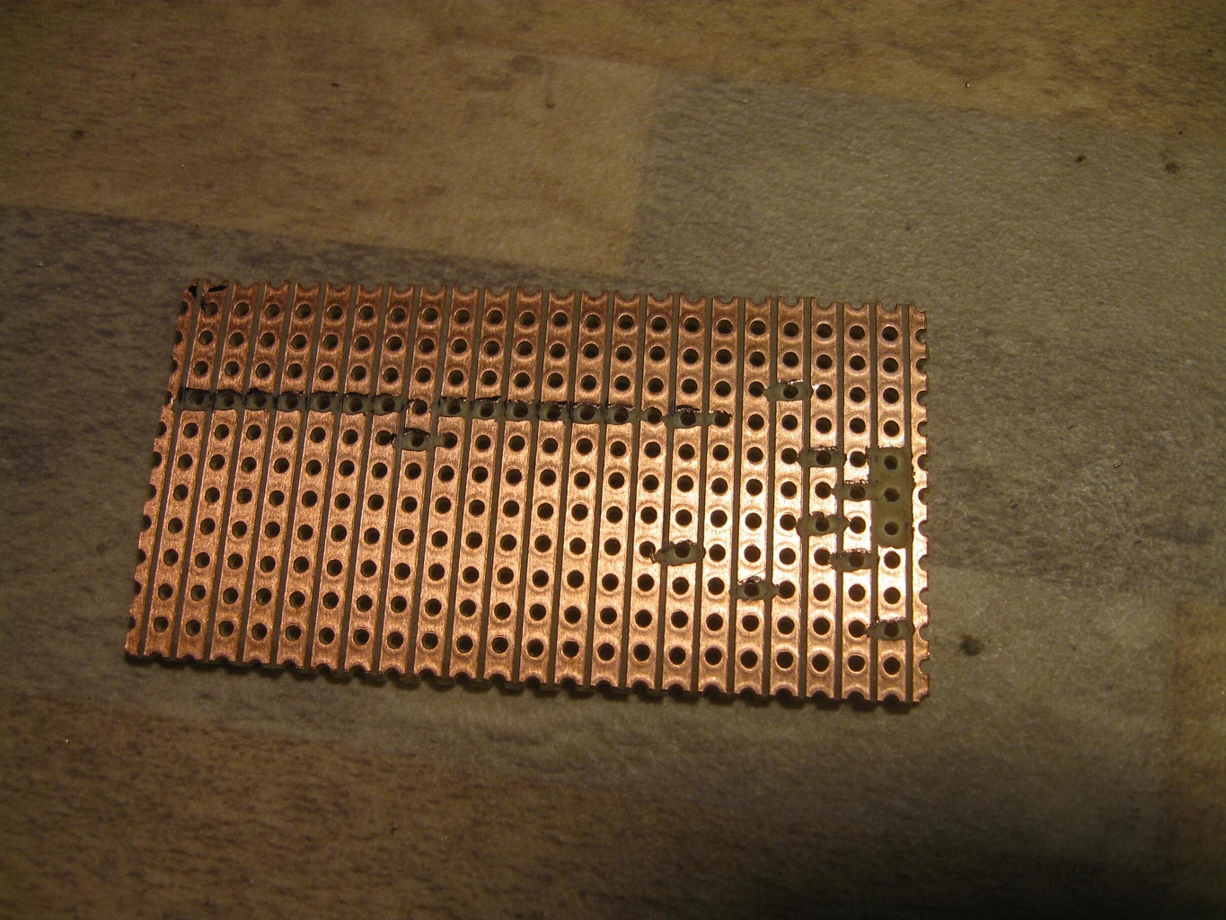
Step 3: Prepare Stripboard
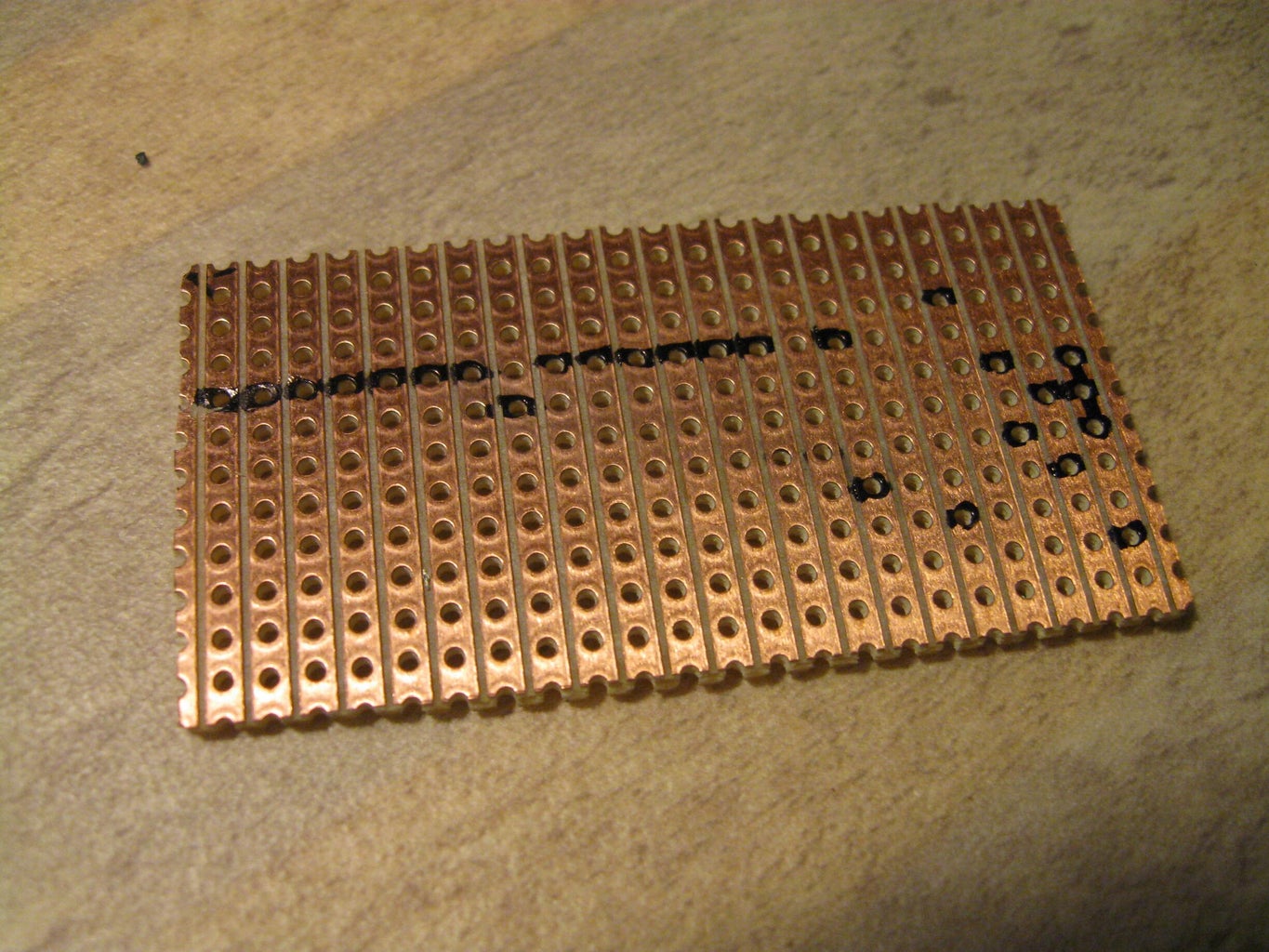
Cut the stripboard in shape – 11 x 22 holes must be intact.
Lay the components on the board and get somewhat familiar to their positions, it would probably make following process easier if you can already take into account how tight you have to work at the end.
Mark the parts of the traces where grey squares are on the drawing. Check your markings once more.
Remove traces according to the marking.
If you make thin cuts then make the cuts in between each hole among these 5 that are under and by the male headers. Also separate the female pin header from crystals legs.
Step 4: Lowest Profile Components


Dropping the IC socket in just for position reference can be helpful.
But first things to lay out and solder are the two resistors and rectifier diode because they are thinner than the socket.
(Actually you can put things on the board in any order you like, but I recommend for sure leave female headers last, because it is much easier to do the wire connections when they are not blocking the access yet.)
Diode has polarity and my images have the polarity wrong – don't be as forgetful as I was. The end with the band is supposed to go towards ATmega socket.
Next two things convenient to put in are IC socket and crystal oscillator. You have to bend the crystals legs inward to fit holes right next to each other and it will be floating not flush with the board. But no problem, it will be protected between headers later.
Step 5: More Components


Add the two 22pF capacitors – one from each leg of the crystal to GND rail. Ground is right next to the crystal. You could just in case drop in the female header for a moment and check how well the capacitors fit between it and the crystal.
Next I added the button. Mouse type buttons have three legs – one on the end is marked C – common, others are NO – normally open, and NC – normally closed. I hope they are placed the same way always. I cut off the NC leg to use the rail under it without mess. We need the normally open part of the switch only.
Next parts to add are 10nF capacitors next to the ATmega. Their purpose is to protect against voltage changes that can disturb processors work. They go between VCC and ground pins and analog reference and ground pins. Some capacitors might also need bending to fit that right-next-hole spacing.
Next add the two remaining 10 nF ceramic capacitors. The purpose of all the capacitors in this circuit except the 100nF ceramic one is to smooth out the voltage, maybe I have been even too generous putting so many, but it sure won't hurt.
And finally the 100nF ceramic capacitor. This one is for decoupling reset pin from FTDI cables corresponding wire. (Uploading programs did not work without this capacitor, but I read that pressing and releasing reset button at the right moment might do the trick if there is a connections instead of a capacitor. I never got the timing right though.) This one is not on most of the images, because I realized it's needed only after my "finished" board did not work.
After the ceramic ones are soldered add the electrolytic capacitor. Pay attention to the polarity – negative side must face the ATmega chip.
LED – again a polarized component. Cathode – that means the side that is cut off and has shorter leg – should be towards the resistor.
Finally male header pins.
Step 6: Wiring

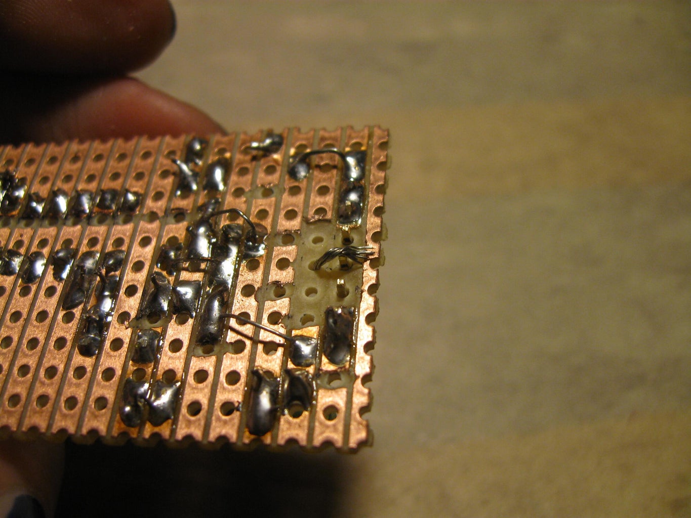


I made bottom wiring before the top one, but it might be more rational to begin on the top. If one hole on the top is hard to reach you can maybe use next one when that is not yet occupied by bottom side jumper. But observe that the electrical connections between components would remain exactly the same if you change the physical layout.
So, top wires it is. Start with the shortest connections. I managed to push most of the wires in between components. That takes also some exact cutting into length effort. Wires on reset, pin 0 and pin 1 should be put in in that order. And it is easier to insert one end, solder it to stay put, then use needlenose pliers if necessary to insert the other end.
Some of the connections to the male header are done so that the wire is stripped longer, inserted through hole next to header and then bent down to touch the header. Then soldered in place. See image about that.
Make the battery clip from old 9V battery or add some other voltage supply connection of your liking. Supply should be between 7 and 12 volts.
When wires on the top side are in place, it is good time to add female headers. You can cut them into pieces of 14, 8 and 4 and skip the crystal rails, or you can use 14 and 14 as I did. I drew the traces to be cut so that the headers would not be attached to crystal and there isn't a hazard of messing something up if you accidentally insert something to these headers.
Now you can do all the bottom wire connections. If you had problem fitting all top wires in the limited space don't be afraid to move some of those to the bottom. Put the printed and folded schematic against a window or glowing computer screen and mark the connections to the other side.
And the last and the tallest component goes into the circuit – 7805 voltage regulator. I bent it's legs somewhat to the side of its radiator to make at least some room between it and the electrolytic capacitor. Heat is not good for that capacitor. See images which way that thing goes in.
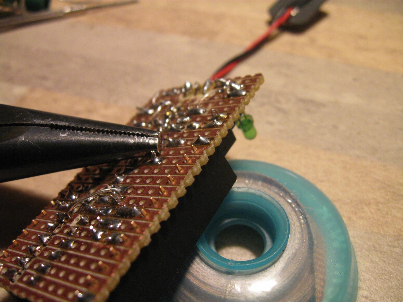
Step 7: Testing

Just connect the battery.
If the LED lights up at normal brightness the power supply part is probably okay.
If not, check
- led polarity,
- rectifier diode polarity,
- wire connections
- other less likely stuff ...
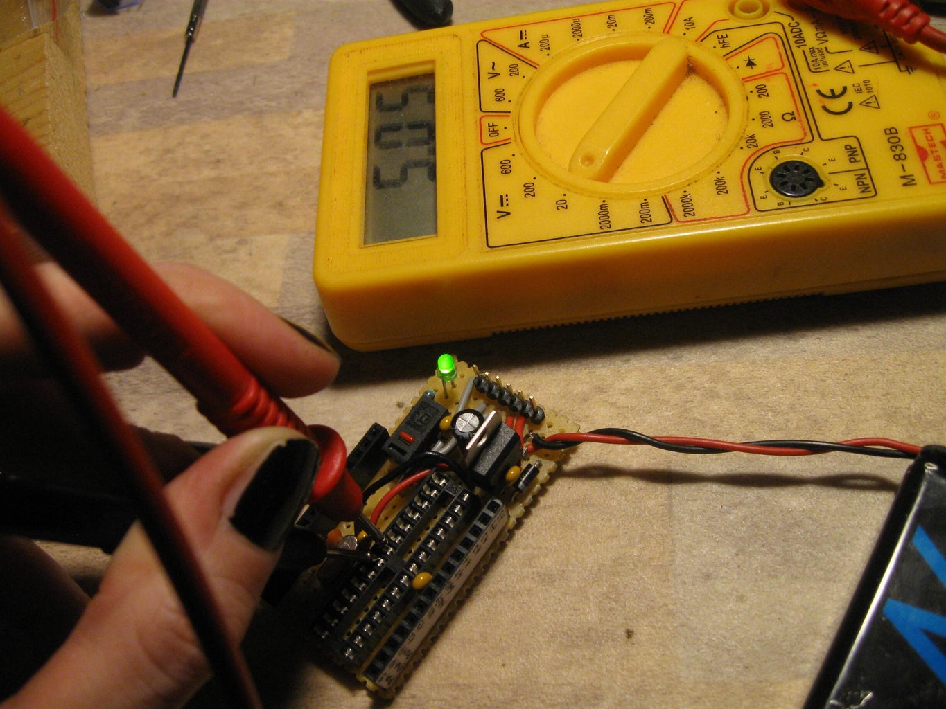
Use multimeter to do some voltage checks on the chip socket. If there is 5V (and not 9 or something) in between each GND and VCC pin?
If not check all wire connections with the help of schematic. There are many connections for VCC and GND lines and easy to make a mistake.
Then keep one multimeter probe on some GND pin and go through all the other pins in the socket. There should also be 5V on RESET but not on any other I/O pin.
If you also want to check the FTDI header connections, remove battery first and measure resistance between male headers and IC socket where the wires go.
If you got that thing working as it should you can insert your ATmega now :)
Step 8: Final Goodies


To avoid shorting things with a random screwdriver lying on you desk I suggest cover up the bottom of the board. I used cardboard wrapped in duct tape and squishy double sided tape for that.
Also to avoid googling for the Arduino ATmega pin layout every time add labels to the pins.
Finally markings for the FTDI cable orientation would not hurt also, even though it is possible to trace the wires if you know FTDI pinout. I used tiny pieces of green and black electrical tape for that (The cable usually has colored wires).
Now get a FTDI cable and breadboard out and do a blink sketch test or something* **
*If you only have an atmega without bootloader, see next step.
**If you are still waiting for an FTDI cable to arrive you might still be able to test your creation with help of usual Arduino too. See step 10.
Information about my FTDI cable is here https://www.instructables.com/id/FTDI-cable/
Step 9: About Burning Bootloader to ATmega

Here is straightforward guide http://arduino.cc/en/Tutorial/ArduinoISP
If your ATmega does not have a letter P right after it's number (as 328P - and “-PU” does not count, only right after the number P matters), then you will get an error, but it is resolvable. You must make a temporary change in one text file. Here is the description of the process:
http://arduino.cc/forum/index.php/topic,68889.msg508969.html#msg508969
The suggestion about duplicating part of that text does not work so simply. Just change it and change back later. And you can leave your own comment into that file for future reference, like so
#------------------------------------------------------------
# Atmega328P
# For Atmega328 change line:
# signature = 0x1e 0x95 0x0F; to
# signature = 0x1e 0x95 0x14;
#------------------------------------------------------------
Then there will be just the problem of finding the right file again ... it's named avrdude.conf
Step 10: About Using Arduino As FTDI Programmer
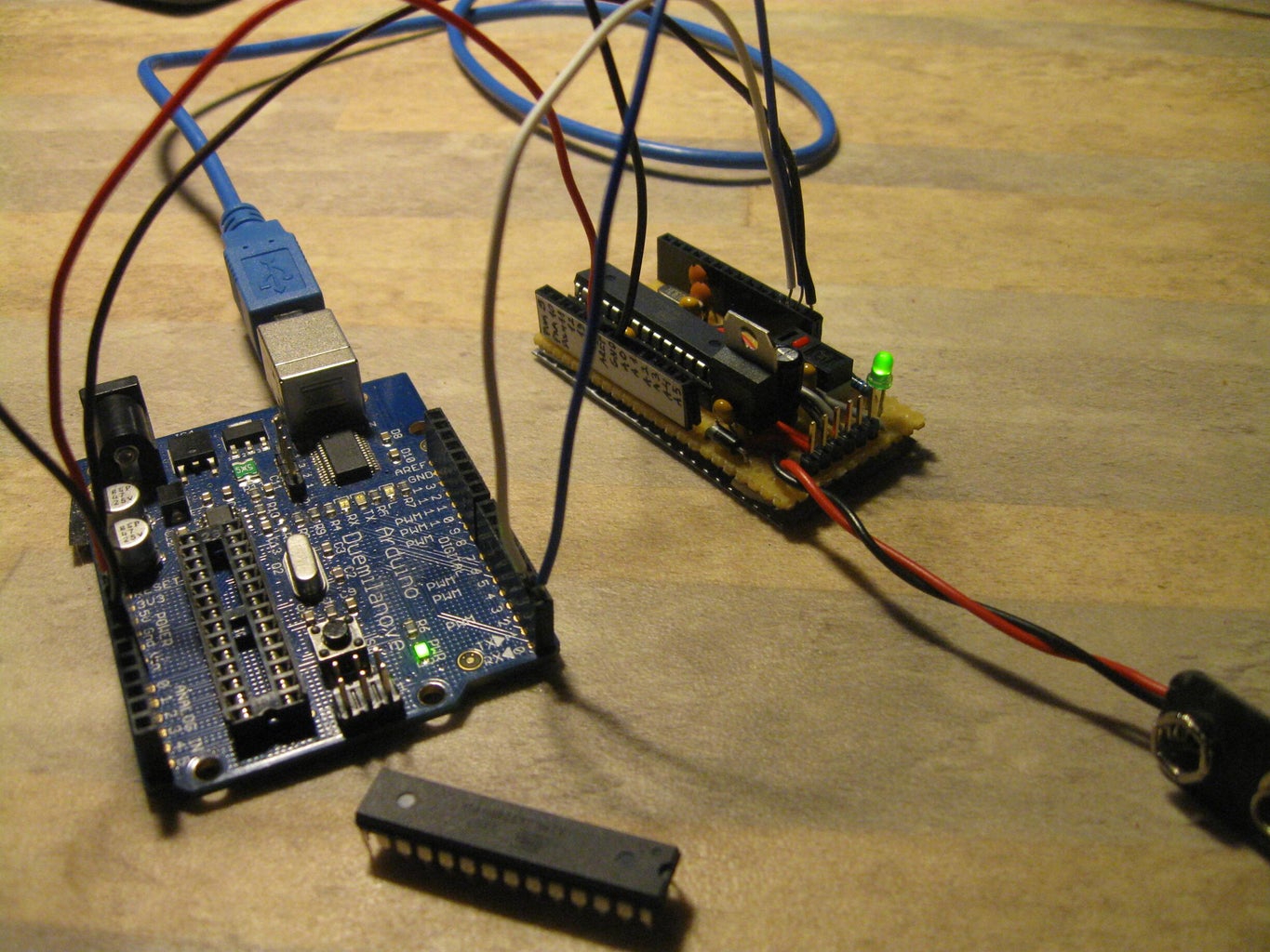
If you do not have an FTDI cable just yet, you can use the built in FTDI part of a regular Arduino board in case you can remove the ATmega chip from it (so Arduino Mega or any other board with soldered controller chip does not work for this). It is no more difficult than burning bootloader was, just the hassle of removing chip. That's why this is not a sustainable solution and you will want that FTDI cable sooner or later.
Here is nice tutorial by member qazwsx755
https://www.instructables.com/id/Arduino-Examples-2-Use-an-Arduino-as-a-FTDI-Progr/


