Introduction: The Altera FPGA and Quartus II Software


This is a step by step walk through of how to set-up and use Quartus software and upload it to the Altera Cyclone FPGA. Done as a primer for my school's(Ivy Tech CC) Digital Fundementals EECT122 course. This will cover in great detail the exact method to setup the software, your design and upload it to the FPGA(Field Programmable Gate Array) board.
Step 1: Open Quartus

Double click the Quartus Icon on the desktop.
Step 2: Folders


Once Quartus opens you will see this screen. Go to the New Project Wizard located in the File tab.
Create a parent folder on your flash drive. You want this on your flash drive because anything saved on the colleges hard-drives may not be there next class.
Create a parent folder where you want to keep all of your Labs! i.e. G:\Joe_Schmo_jumpdrive\EECT122\
Next:
Create a child folder this particular lab will be stored. i.e. G:\Joe_Schmo\EECT122\Lab_1-1\
You can do this either in windows explorer or directly in the program Quartus. IMPORTANT!!!!:
VERY IMPORTANT!!!!!!!!!:
For quartus to work right, your build files(.bdf/.vhd/.etc) need to be in a folder(your child folder) that has the same name as the projects.
Step 3: New Project Wizard

Wizards are great aren't they? This one guides you through the initial setup of your project. After selecting the appropriate name of your parent folder and creating an appropriate child folder, it's time to name your project. You want to call it "I rock Ivy Tech EE" I know. But if you do that and it doesn't match the child folder you've create, the software will get really confuses later on. Just name your project the EXACT same thing as the child folder. In the picture below it is "tutorial." And so EVERY different type of file in this project will get named "tutorial."
tutorial.bdf
tutorial.vdl
turorial.etc
After that's done, click next.
Step 4: Add Files

Do you want to add files. Well for our purposes NO. Click next without hitting anything.
Step 5: Select the Right Board


In this class we are using the Cyclone II EP2C20F484C7.
Step 6: EDA Tools?

You don't need any tools. Hit next.
Step 7: Finish Your Set Up

Everything look right?
Well hit finish and lets get started programming a FPGA.
Step 8: Block Diagram/ Schematic


We will now begin to enter gates and create a schematic "program" to be executed on the hardware development board.
Go to the FILE tab and hit New. Here you will have the option to create many different types of files. For this tutorial we will be creating a Block Diagram/Schematic File.
Step 9: Save the File

It is highly recommended that you save the file at this time. Remember, this file name " *.bdf " must be the same name as the folder that was created earlier on. Steps 1 though 8 go about created other files that are needed for everything to work properly and if this ".DBF" (Diagram-Block) file does not live in that same folder, it won't work right.
So for this example I saved it as "G:\tutorial.bdf
Step 10: Create a Schematic


Now the fun part begins. This is where we create the schematic. On the left of this new window are various tools you can use to add logic gates and other parts to complete your project. You are able to turns wires into buses, add text, zoom in and out, and many other things through the buttons on the left.
The third picture in this series shows a diagram of a 4 bit comparator that was created rather quickly.
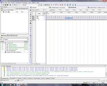
Step 11: Start Compilation


Just like written code, schematic diagrams must be compiled into machine code for it to be used. Also like writing programming language, this is where you get error and must debug things. The error messages provided by Quartus tend to be much more useful than other messages from IDE compilers.
Up at the top tool bar, the button that looks like play button will start the compilation.
You can also navigate to the "Processing Tab" and hit "Start Compilation".
Step 12: Save

If you are successful your screen will look similar to image 2.
You must save the compiled BDF before proceeding to create a Vector Waveform.
Step 13: Vector Waveforms


So you've wired some virtual chips together and it works. Now it's time to see what the output actually is and determine if it's what was expected. To do that we are going to use a Vector Waveform file.
Under the File tab, select New, and then Vector Waveform file.
This screen should look familiar, it is the same place where we created the Block Diagram file.
Step 14: SAVE

Once again, Immediately after creating the new vector waveform file, Re-save it with the SAME name as the parent folder.
So for this tutorial it is saved as "G:\Joe_Schmo\EECT122\Lab_1-1\tutorial\tutorial.VCF"
Step 15: Setting Up the Waveform File-End Time


Typically, this window pops up with a total time to analyse the output of your circuit of 20 nanoseconds. That is a little short on time. We will change this by navigating to the Edit tab, and selecting End Time.
In this class, 16 micro-seconds will be a nice time frame to work with. Some labs might specify a different time, this is where you change that.
Step 16: Setting Up the Waveform File-Edit Grid Size


The grid size doesn't automatically change. So want to change it. Under the Edit tab, click Grid Size.
Inside the dialogue window, edit the boxes and double check that you have selected the right scale(nano, micro, milli).
After the settings are correct, Use the keyboard shortcut and press CTRL W to view the entire timeline. It should look like picture 3.
Step 17: Add Inputs and Outputs


Now that the vector file is configured properly we need to import or link to the inputs and outputs created in our Schematic file.
Right click on the left panel. Scroll down to INSERT and over to INSERT NODE OR BUS.
This will bring up a new window with several options. Underneath the cancel button, is a button called NODE FINDER. Press that button and leave the other options alone.
This brings up a new window called NODE FINDER.
----At the top middle, scroll down and select "Pins: All"
----next, over to the right is a button that says list. It searches for the pins in your schematic. Hit that button.
----Once pins are in the left tab, we need to select them. This can be done individually if needed with the single arrow button, or all pins at once with the double arrow button.
-----Lastly, Click OK in the "Node Finder" window and also OK in the "Insert Node or Bus" window.
Step 18: Simulating


This simulation will run your circuit and easily allow you to change the inputs. This was our whole goal.
The first two pictures show my comparator circuit will no inputs. Both data streams here A and B have no data, thus they are equal and the "W" output goes high.
The next few pictures will show how to change the input and what happens to the output "W" when the two data streams are not equal.
Step 19: Changing the Input of the Circuit.


- Right click the input on the left hand column.
- Scroll down to Value and over to Count value or some other value(Like Clock).
- Shown is "count value." I will use Hex for this purpose
- This brings up a pop-up with option for how much to count by and when to count by. (Change time and value)
- Do the same thing for the "B" data stream.
- No highlight a few clock cycles and you can manually change them by right clicking on the highlighted area and selecting the value.
- Notice in this last picture that the two data stream are now no longer equal.
- And the result is a low where the two data streams do not match up.
Step 20: Download to Board

- First thing is to assign to the pins on the Alterra board that we are going to use. For this example we need 8 input pins and one output indicator. The DOC attached to this step has the Alterra pin assignments.
Attachments

Step 21: Pin Planner


Go to the Assignments tab and down to Pin Planner.
This brings up a new window. Go ahead and maximize it.
Step 22: Pin Planner 2


In this pin assignment window, you can select the individual pins by clicking in the location field and typing or searching for the correct pins.
Step 23: Get It on the Board


This last step is the easy one.
Go to TOOLS and down to Programmer.
This will bring up a new window; check to make sure it says Blaster and click Start.
Congrats you're Done.