Introduction: Making a Hand Drawn PCB.


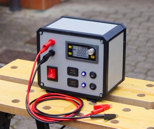
For my latest electronics project I decided to make a resistor substitution box, instead of just using another perf-board I decided to make a pcb for it so I could document the process and make an instructable. I decided to do this because I have yet to see anyone do it on Instructables so I figured it would be a good thing to share. This process works well for simple circuits that do not have a lot of small parallel bus lines in them, I have done a few guitar stomp boxes this way as well.
Step 1: Materials


Materials to design and Draw the board:
-Paper and Pencil
-Ruler
-Sharpee
-Tape
-Scissors
-Tiny #65 twist bit (0.035" which is good for most electronic components)
-Dremal or pin vise to drill holes, the Dremal is the obvious winner here
-Copper clad PC board
Materials to etch the board:
-Ferric Chloride(FC), which is used to etch the board
CAUTION Ferric Chloride is a very corrosive liquid the vapor well cause steel to rust, therefor one must take all precautions nessessery in order to protect yourself as it well cause nasty burns and alike. So therefore you well also need
-Rubber Gloves
-Safety Glasses
-Paper towels to clean up spillage
-A well ventalated work area as the vapor is also quite nasty and not good to breath in.
Aside from all the safety stuff you need,
-A small resealable plastic container to put the FC into for etching and storage afterwards.
-A larger plastic container that the small one well go into for water and storage of materials afterwards.
-Warm water, goes in larger container to heat the FC.
Step 2: Designing the Circuit

Using paper and pencil design the layout of the circuit, it is easiest to do this as a top view of the board, it helps to also have all the different components on hand to help with spacing and placement. As a side note also make sure to design the layout so that it well fit on the board. If you already have a pre-designed layout you can skip this part.
Here is what my layout looks like for the resistor substitution box.
Step 3: Drilling the Board.


-Next you well want to make a copy of the design that is a reverse of the original, if you drew it in reverse or the one you have is already reversed just make a regular copy of it.
-Cut the copy of the layout out with scissors leaving some on either side so you can fold it around the PCB and tape it in place.
-Now using the tape, tape the design onto the copper side of the PCB. Mine is on the other side because I did not bother to make a reversed copy of it.
-With the #65 drill bit use the layout to drill a hole in the center of all the solder pads for the individual components. I like to set the board over something to catch the small fiberglass dust generated by the drilling, in this case a small glass dish.
Step 4: Drawing the Traces


-After you have drilled all the holes remove the copy of the design from the PCB and clean off all the dust.
-Using the Sharpie draw a solder pad around all the holes you drilled, helps to have a fresh pen with a sharp point for this, make sure the pen leaves a nice bold line otherwise it well not resist the FC as well.
-Now using the reversed copy of the layout as a reference draw in all of the traces with a Sharpie, if you make a mistake you can use alcahol on a bit of paper towel to erase the error.
-You can also use the Sharpie to add text to the board for connections or whatever.
-If you have not done so already, cut your board(s) out from the rest of the PCB stock.
Step 5: Etching


-Start off by finding a clean dry place where you can safely etch the circuit board, preferably outside.
-Put gloves and safety glasses on.
-Make sure you put your gloves and safety glasses on, Ferric Chloride is nasty stuff.
-Take your small container and pour about 1/4" to 1/2" of Ferric Chloride into it.
-Fill the larger container with warm water about 1" deep.
-Drop PCB into the Ferric Chloride, copper side up and place the small container into the water in the larger container.
-Gently rock the small container in the water so as to keep the FC moving which helps with the etching process.
-In about 5-7 minuites you should start to see the copper start to desolve away, notice the areas where the traces a drawn are uneffected.
-After about 10-12 miniutes the board should be completely etched, at which time you should emmediatly remove the PCB and drop it into the water in the larger container to rinse it and then dry it off on the paper towel.
-When you are done put the cover on the small container, you can use the Ferric Chloride over again a few times, and pour out the water in the larger container and rinse it out. You can use the larger container to store the small container and your extra Ferric Chloride that is still in the original bottle.
Step 6: Cleaning the PCB

-Using 0000 Steel wool clean the Sharpie off the the traces.
-Populate the board with components.