Introduction: 555 Timer


This tutorial provides sample circuits to set up a 555 timer in monostable, astable, and bistable modes as well as an in depth discussion of how the 555 timer works and how to choose components to use with it. The 555 timer is a chip that can be used to create pulses of various durations, to output a continuous pulse waveform of adjustable pulse width and frequency, and to toggle between high and low states in response to inputs. By wiring the 555 timer with resistors and capacitors in various ways, you can get it to operate in three different modes:
Monostable Mode is great for creating time delays. In this mode an external trigger causes the 555 timer to output a pulse of an adjustable duration. Jump straight to an example circuit for monostable mode here.
Astable Mode outputs an oscillating pulse signal/waveform. In this mode the output of the 555 timer is switching between high and low states at a tunable frequency and pulse width. Jump straight to an example circuit for astable mode here.
Bistable Mode causes the 555 timer to toggle its output between high and low states depending on the state of two inputs. Jump straight to an example circuit for bistable mode here.
Some applications that come to mind include:
- a steady clock/trigger to keep time in a circuit (astable mode)
- the core oscillator of an analog synthesizer, with the addition of some op amps and other components this pulse wave can be shaped into a triangle, saw, and even sine shapes
- a very basic chiptune style noise maker (see atari punk console)
- time delay for an incoming signal (monostable mode)
- very basic storage of input data/management of two button control system (bistable mode)
The 555 timer is flexible, cheap, and easy to find (you can even pick them up at Radioshack). It's also a great starting point for audio projects because its output can be wired directly to a speaker.
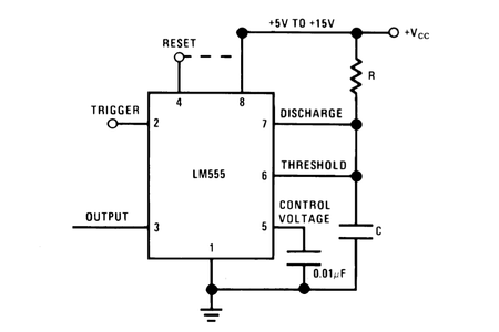
Step 1: 555 Timer Pin Diagram


Fig 1 shows the pin connections to the 555 timer, it was take directly from the 555 timer datasheet. The power connections to the chip are through pins 1 (ground) and 8 (+Vcc). The positive supply voltage (+Vcc) should be between 5 and 15V.
The second image is a close up of the diagram depicting the internal functional components of the chip. This consists of a few different elements: resistors, transistors, comparators, a flip flop, and an output stage.
All three resistors diagrammed in fig 2 are 5kOhm (see image notes in fig 3). The purpose of these resistors is to set up a voltage divider between Vcc and ground. Since all resistors are the same value we know that the voltage at the junction between the resistors are 2/3Vcc and 1/3Vcc (see image notes in fig 2). These voltages are used as reference voltages for the comparators.
A comparator is a circuit which compares an input with a reference voltage and outputs a LOW or HIGH signal based on whether the input is a higher or lower voltage than the reference. The 555 timer uses several transistors to construct its comparators (see the image notes in fig 3), so in the simplified functional diagram in fig 2 they are represented by boxes labelled "comparator." The comparator connected to pin 2 compares the "trigger" input to a reference voltage of 1/3Vcc and the comparator connected in pin 6 compares the "threshold" input to a reference voltage of 2/3Vcc from the voltage divider.
A flip flop is circuit that switches between two stable states based on the state of its inputs. The 555 flip flop outputs a high or low based on the states of the two comparators. When the trigger comparator is outputting a low signal (regardless of the state of the threshold comparator), the flip flop switches high, when both comparators are outputting a high signal, the flip flop switches low. The timing of a high pulse output from the flip flop can also be manually reset (the beginning of a pulse can be triggered) by pulsing the reset pin low.
The functional diagram in fig 2 also includes two transistors. The transistor attached to pin 7 is an NPN transistor. Since pin 7 is connected to the collector pin of the NPN transistor, this type of configuration is called open collector or open drain. This pin is usually connected to a capacitor and is used to discharge the capacitor each time the output pin goes low. The transistor attached to pin 4 is a PNP transistor. The purpose of this transistor is to buffer the reset pin, so the 555 does not source current from this pin and cause it to sag in voltage.
The output stage of the 555 timer is indicated in the image notes of fig 3. Its purpose is to act as a buffer between the 555 timer and any loads that may be attached to its output pin. The output stage supplies current to the output pin so that the other functional component of the 555 timer don't have to.
Step 2: 555 Timer: Monostable Mode
In monostable mode the 555 timer outputs a high pulse, which begins when the trigger pin is set low (less than 1/3Vcc, as explained in the previous step, this is enough to switch the output of the comparator connected to the trigger pin). The duration of this pulse is dependent on the values of the resistor R and capacitor C in the image above.
When the trigger pin is high, it causes the discharge pin (pin 7) to drain all charge off the capacitor (C in the image above). This makes the voltage across the capacitor (and the voltage of pin 6) = 0. When the trigger pin gets flipped low, the discharge pin is no longer able to drain current, this causes charge to build up on the capacitor according to the equation below. Once the voltage across the capacitor (the voltage of pin 6) equals 2/3 of the supply voltage (again, as explained in the previous step, this is enough to switch the output of the comparator connected to pin 6), the output of the 555 is driven back low. The output remains low until the trigger pin is pulsed low again, restarting the process I've just described.
(Voltage across Capacitor) = Vcc * (1- e-t / (R*C))
this equation describes the time it takes to charge a capacitor of capacitance C when it is in series with a resistor of resistance R
as explained above, we are interested in the time it takes for the voltage across the capacitor to equal 2/3Vcc, or:
2/3*Vcc = Vcc * (1- e^-t / (R*C))
which can be rearranged to:
2/3 = 1- e-t / (R*C)
e-t / (R*C) = 1/3
-t / (R*C) = ln(1/3)
t = 1.1*R*C seconds
In the next step I'll connect an indicator LED to the output pin of the 555 and pick some arbitrary values for R and C to make sure that this really works.
Step 3: 555 Timer: Monostable Mode Circuit


As I explained in the last step, a 555 timer in monostable mode will output a high pulse (of voltage ~Vcc) when the trigger pin in pulsed low. The duration of this output pulse is dependent on the values of R and C in fig 4. In the last step we calculated the duration of the pulse output from the 555 in monostable mode to be:
t = 1.1*R*C seconds
where R and C are the resistor and capacitor in series in fig 4.
if we choose R = 10Kohms and C = 470uF
t = 1.1*10000*0.00047
t = 5.17 sec
This means that with a 10Kohm resistor and 470uF capacitor, a pulse low to the 555's trigger pin (pin 2) will cause the output to go high for 5.17 seconds.
I built a circuit which connects the output pin of the 555 to an LED, causing the LED to light up for the duration of the pulse. This way I would have a visual indication that my calculations were correct. I connected the trigger pin of the 555 to a push button momentary switch, connecting it to ground when pressed. Photos of the circuit are shown above, and the schematic is shown in fig 5.
Parts List:
555 timer Digikey LM555CNFS-ND
0.01uF capacitor Digikey 445-5297-ND
470uF capacitor Digikey P5185-ND
(x2) 10Kohm resistor Digikey CF14JT10K0CT-ND
470 ohm resistor Digikey CF14JT470RCT-ND
amber led Digikey C503B-ACN-CW0Y0251-ND
momentary switch Digikey CKN9018-ND
22 gauge jumper wire
breadboard Amazon
5-15V power supply- if you don't have a bench power supply, try using a 9V battery and battery snap or use the 5V output from an Arduino
Wiring Info:
The schematic is shown in fig 5. Connect power and ground to pins 8 and 1 of the 555 timer (red and black wires). I used a 9V supply and battery snap for my circuit. As indicated in the schematic in fig 5, connect a 0.01uF capacitor between pins 5 and 1. Connect a 440uF capacitor between pins 1 and 6, make sure that the negative lead of the capacitor is connected to pin 1. Connect pins 6 and 7 with a jumper wire (green). Connect a 10K resistor between pins 7 and 8. I left the reset pin floating, you could connect it to Vcc as well.
Connect an LED and current limiting resistor in series from the output of the 555 to ground. The output pin of the 555 will output Vcc-1.2V maximum (the -1.2V comes from some transistors in the circuit that drop the voltage slightly). My circuit was driven by a 9V supply, so the max output is 9-1.2V = 7.8V. I used a 470ohm current limiting resistor for my setup, if you use a 5V supply you can use a lower current limiting resistor (like 220ohm), and for higher Vcc use a higher resistance (maybe even up to 1K).
Wire the momentary push button switch in series with a 10K resistor between Vcc and ground. Connect a wire (yellow) from the junction between the switch and resistor to the trigger pin so that when the switch is not pressed the trigger pin is held high. When the switch is pressed the trigger pin will drop to low. See the schematic if this does not make sense.
Operation:
Press the button. The LED should light up for a time and then turn off. If you time the LED, you'll find that it lights up for exactly 5.17 seconds, just as I calculated above.
You can experiment with switching out the 10k resistor or the 470uF capacitor (connected to the 555) to see how they affect the duration of the output pulse. Remember, since t = 1.1*R*C seconds, increasing resistance or capacitance will always increase the duration of the pulse.
I wired up a 10Kohmpotentiometer as a variable resistor and put it in my circuit in place of the 10K resistor between 555 pins 7 and 8 (fig 9). This way by turning the knob all the way to one side, the LED stays on for 5.17 seconds, but when turned to the other extreme the LED turns off immediately after I released the button. Turning the potentiometer to any position in between will cause a pulse duration anywhere from 0 to 5.17 seconds.
Step 4: 555 Timer: Monostable Mode (Fast Applications)


in the step 2, we calculated the time of the high pulse from the 555 timer for a given R and C
t = 1.1*R*C seconds
so if we choose R = 5.1Kohms and C = 1uF
t = 1.1*5100*0.000001
t = 5.61 ms
Since this pulse is happening on a much faster time scale then in the last step, I used an Arduino to pulse pin 2 of the 555 timer low every 10 ms and measured the output of the 555 on an oscilloscope. Here's how I set it up:
Parts List:
555 timer Digikey LM555CNFS-ND
0.01uF capacitor Digikey 445-5297-ND
1uF capacitor Digikey P5174-ND
5.1Kohm resistor Digikey CF14JT5K10CT-ND
22 gauge jumper wire
breadboard Amazon
5-15V power supply- if you don't have a bench power supply, try using a 9V battery and battery snap or use the 5V output from an Arduinopulse generator- I used an Arduino for this
oscilloscope
Wiring Info:
Figs 1-3 show how I connected the 555 up on a breadboard. Connect power and ground to pins 8 and 1 of the 555 timer (red and black wires). I used a 9V supply and battery snap for my circuit. As indicated in the schematic in fig 4, connect a 0.01uF capacitor between pins 5 and 1. Connect a 1uF capacitor between pins 1 and 6, make sure that the negative lead of the capacitor is connected to pin 1. Connect pins 6 and 7 with a jumper wire (green). Connect a 5.1K resistor between pins 7 and 8. I left the reset pin floating.
I used an Arduino to trigger a low pulse every 10ms to pin 2 of the 555 timer. You could also use a function generator to generate this pulse signal. Here's the code I used:
<pre>//555 timer trigger- monostable mode
//by Amanda Ghassaei
//Sept 2012

//pin connections:
//digital pin 0 to 555 pin 2
//Arduino ground to 555 ground (pin 1)

void setup(){
  pinMode(0,OUTPUT);
  digitalWrite(0,HIGH);
}

void loop(){
  //pulse pin 0 low momentarily
  digitalWrite(0,LOW);
  digitalWrite(0,HIGH);
  delay(10);//wait 10 ms
}
Connect the signal out (digital pin 0) to 555 pin 2 (yellow) and ground (of the Arduino or the function generator) to 555 pin 1 (black).
Operation:
Fig 5 shows the output from the 555 timer. You can see that the duration of the high pulse is about 5.6ms, as expected. Also notice how a new pulse is triggered every 10 ms, each time the signal from the Arduino drops low. Fig 6 shows the output from the 555 in blue and the output from Arduino digital pin 0 in yellow. You can see that the Arduino signal is normally high, it drops low for a tiny fraction of a second, only visible when we zoom in the time/div in figure 7. In fig 7 you can see that the signal from the Arduino drops low for less than 5us and the output from the 555 immediately goes high. Fig 8 shows the output from the 555 in blue and the voltage across the 1uF capacitor (also the voltage of pin 6). Notice how the output from the 555 timer drops low when the voltage across the capacitor = 2/3Vcc (in this example I'm using a 9V battery supply, so 2/3Vcc = 6V). When the output from the 555 drops low, it causes the discharge pin (pin 7) to rapidly discharge the 1uF capacitor. Fig 9 shows a closeup of this discharge happening, you can see the voltage across the capacitor drop from 2/3Vcc to 0 in about 50us.
For comparison, in figs 10 and 11 I set up another 555 timer on my breadboard, identically to the setup of the first 555, but I used a 0.47uF capacitor instead of a 1uF. I calculated the duration of the pulse for this new circuit:
t = 1.1*R*C seconds
t = 1.1*5100*0.00000047
t = 2.64 ms, approximately half of the duration of the first 555 timer pulse.
Fig 12 shows the output from both 555 timers on the oscilloscope: the 1uF circuit in blue, and the .47uF circuit in yellow. You can see that the duration of the pulse from the second (0.47uF) 555 timer is about 2.6ms, as calculated above. Also notice how even though the output pulses have different durations, both pulses start at the same time, right when the Arduino pulses their trigger pins low. This use of monostable mode with an external trigger is an effective way of controlling the pulse width (the duration of the high pulse) of your output signal. By replacing the resistor with a variable resistor, you can tune the pulse width to whatever you want. You can change the frequency of the pulse waveform by changing the frequency of your external trigger. I'll also introduce another way of creating a pulse width modulated signal without an external trigger using astable mode in step 7.
Step 5: 555 Timer: Astable Mode

In astable mode, the output from the 555 timer is a continuous pulse waveform of a specific frequency that depends on the values of the two resistors (RA and RB) and capacitor (C) used in the circuit (fig 1) according to the equation below. Astable mode is closely related to monostable mode (discussed in step 2), you can see that the schematic is nearly the same. The important difference is that in astable mode, the trigger pin is connected to the threshold pin; this causes the output to continuously toggle between the high and low states.
Frequency of Output = 1/[0.7*(RA+2*RB)*C]
(don't worry, I'll demonstrate how I derived this equation soon)
The sequence of events is somewhat complex, so I've broken it down into 5 steps:
1. Initially there is no charge on the capacitor C, so the voltage across the capacitor is zero. The voltage across the capacitor C is equal to the voltage at pins 6 (threshold pin) and 2 (trigger pin) since they are all connected. So initially the threshold and trigger pins are both at zero volts as well. This drives the output high.
2. As explained in step 2 of this Instructable, when the trigger pin is low it renders the discharge pin unable to drain charge off the capacitor. Since the capacitor C is in series with RA and RB and Vcc is being applied, current will flow through the resistors and start to accumulate charge on the capacitor. This causes the voltage across the capacitor C to increase according to the following equation:
(Voltage across Capacitor) = (Vcc - V0) * (1- e-t / [(RA+RB)*C])
where "Voltage across Capacitor" is the current voltage across the capacitor at time t, V0 is the initial voltage across the capacitor, Vcc is the total voltage applied to the resistors RA, RB, and the capacitor C
3. When the voltage across the capacitor C equals 2/3Vcc it causes the threshold pin to register as high (as explained in step 1 of this instructable, this flips the comparator attached to the threshold pin inside the 555). This drives the output low and enables the discharge pin. The time it takes for a voltage of 2/3Vcc to accumulate on the capacitor is given by:
2/3*Vcc = (Vcc - V0) * (1- e-t / [(RA+RB)*C])
2/3*Vcc/(Vcc - V0) = 1- e-t / [(RA+RB)*C]
1/3*Vcc/(Vcc - V0) = e-t / [(RA+RB)*C]
ln[1/3*Vcc/(Vcc - V0)] = -t / [(RA+RB)*C]
t = -(RA+RB)*C*ln[1/3*Vcc/(Vcc - V0)]
for V0 = 0V, this comes out to:
t = 1.1*(RA+RB)*C seconds
4. With the discharge pin enabled, charge starts flowing off the capacitor, through RB, and into the discharge pin of the 555. This lowers the voltage across the capacitor as described by the equation below:
(Voltage across Capacitor) = (Peak Voltage Across Capacitor) * ( e-t /(RB*C))
where the peak voltage across the capacitor was the voltage just before the discharge pin was enabled: 2/3Vcc
(Voltage across Capacitor) = 2/3*Vcc* ( e-t /(RB*C))
5. Once the voltage across the capacitor (and the voltage at the trigger pin) equals 1/3Vcc, the trigger pin registers as low (as explained in step 1 of this instructable, this flips the comparator attached tot he trigger pin inside the 555). The time it takes for this to happen is solved below. This drives the output high and brings us back to step 2 (above). From here, steps 2-5 repeat forever and the output switches between the high and low states to produce a continuous pulse wave. The time it takes to discharge he capacitor from 2/3Vcc to 1/3Vcc is given below:
1/3*Vcc = 2/3*Vcc* ( e-t /(RB*C))
1/2 = e-t /(RB*C)
ln(1/2) = -t /(RB*C)
t = -RB*C*ln(1/2)
t = 0.7*RB*Cseconds
To calculate the frequency of this oscillation we first calculate the time that the the output is in the high and low states. The output is in the high state while the capacitor charges from 1/3Vcc to 2/3Vcc. The time it takes to charge the capacitor from voltage V0 to 2/3Vcc is repeated below:
the output is high for:
t = -(RA+RB)*C*ln[1/3*Vcc/(Vcc - V0)]
in step 3 (above) we chose V0 = 0 as our initial conditions, but this is true only for the first cycle of astable mode. For all subsequent cycles the capacitor will only discharge to 1/3Vcc before the discharge pin is disabled and charge begins to build on the capacitor again. So we set the initial voltage to 1/3Vcc:
t = -(RA+RB)*C*ln[1/3*Vcc/(Vcc - 1/3Vcc)]
t = -(RA+RB)*C*ln(1/2)
t = 0.7*(RA+RB)*Cseconds
As we calculated above, the output is low for:
t = 0.7*RB*C seconds
So the total duration of both the high and low states of the output is:
0.7*(RA+RB)*C + 0.7*RB*C
0.7*(RA+2*RB)*Cseconds
Then the frequency is calculated as follows:
Frequency of Output = 1/[0.7*(RA+2*RB)*C]
So by changing the values of the resistors RA and RB and the capacitor C, we can control the frequency of the output. Additionally, we can control the pulse width of the output (the duration of high compared to the duration of low) because the duration of the high state depends on both RA and RB, while the duration of the low state only depends on RB. In the next step I'll introduce a sample circuit for astable mode.
Step 6: 555 Timer: Astable Mode Circuit


As I described in the last step, setting the 555 timer up in astable mode causes it to output a continuous series of pulses. In this circuit, I'll set up the 555 timer to output a pulse wave with a frequency inside the audible range, this way I can connect the output to a speaker and hear the results.
Parts List:
555 timer Digikey LM555CNFS-ND
0.01uF capacitor Digikey 445-5297-ND
100kOhm linear taper potentiometer Digikey 987-1300-ND
10kOhm 1/4watt resistor Digikey CF14JT10K0CT-ND
0.47uF capacitor (or anything between 10uF and 0.1uF should be fine) Digikey P5173-ND
speaker
22 gauge jumper wire
breadboard Amazon
5-15V power supply- if you don't have a bench power supply, try using a 9V battery and battery snap or use the 5V output from an Arduino
Wiring Info
The schematic is shown in fig 6. Connect power and ground to pins 8 and 1 of the 555 timer (red and black wires). I used a 9V supply and battery snap for my circuit. As indicated in the schematic in fig 6, connect a 0.01uF capacitor between pins 5 and 1. Connect a 0.47uF capacitor between pins 1 and 6, make sure that the negative lead of the capacitor is connected to pin 1. Wire a 10kohm resistor between pin 6 and 7. Wire a 100K potentiometer wired as a variable resistor between pins 7 and 8. Use jumper wire to connect pins 4 and 8 to each other (red) and pins 2 and 6 to each other (yellow).
Attach the positive lead of a speaker to pin 3 of the 555 and connect the negative lead to ground (pin 1).
Operation
When you power this circuit you should begin to hear the pulse waveform coming from the 555. Turn the potentiometer to change the frequency of this pulse wave. If you want to generate a particular frequency, try changing the values of RA, RB, and C according to the following equation (derived in the last step):
Frequency of Output = 1/[0.7*(RA+2*RB)*C]
where RA, RB, and C are shown in fig 7
Based on the components I used in this sample circuit, we can calculate the range of possible output frequencies as follows:
assuming the potentiometer is turned all the way to one side and the resistance = 100kohms
Frequency of Output = 1/[0.7*(100,000+2*10,000)*0.00000047]
Frequency of Output =~ 25Hz
this output is shown on an oscilloscope in fig 8
Low values of RA should be avoided because they prevent the 555 timer from discharging the capacitor C normally. When I turned the pot all the way to the other side (for a resistance of 0ohms) the 555 timer stopped working as expected (fig 10). So let's calculate the output frequency from the timer when the pot is turned to its halfway point, for a resistance of 50Kohms.
Frequency of Output = 1/[0.7*(50,000+2*10,000)*0.00000047]
Frequency of Output =~ 43Hz
this output is shown in fig 9 (note- there is some error bc I was guessing at where halfway was)
Also notice that although the frequency of the output changes between figs 8 and 9, the duration of the low output phase does not change significantly. This is because the duration of the low output phase is not dependent on RA (the variable resistor). As calculated in the last step:
t = 0.7*RB*C
substituting RB = 10kOhms and C = 0.47uF you get:
t =~ 3ms
which can be verified in figs 8 and 9.
Step 7: 555 Timer: Astable Mode Duty Cycle


The duty cycle of a pulse wave is the ratio of the time it spends high to the total duration of the high and low state. We calculated these durations in step 5, and we can combine them to calculate the duty cycle of the 555:
duty cycle = (time spent high) / (total time duration of high and low states)
substitute the equations from step 5 to get:
duty cycle = (0.7*(RA + RB)*C) / (0.7*(RA+2*RB)*C)
this simplifies to:
duty cycle = (RA+ RB) / (RA + 2*RB)
In the equation above, when RA is much larger than RB (you can ignore the RB terms) you end up with a duty cycle ~= 1 and when RB is much larger than RA (you can ignore the RA terms) you get a duty cycle =~ 1/2. So the limits of the duty cycle with the circuit shown in fig 2 are 50% to 100%. If you wanted to get a duty cycle that was less than 50%, you have to use a circuit like the one shown in fig 1. In this circuit a diode bypasses RB during the charging phase of the 555 (while the output is held high). So how does this affect the durations of the high and low phases of the output?
The duration of low output remains:
t = 0.7*RB*C seconds
this happens when the capacitor is discharging, so current is flowing from the capacitor, through RB (in the upwards direction in fig 1), and into the discharge pin of the 555. This is the opposite direction of current flow that the diode will accept, so no current flows through the diode. During this time, the circuit in figure 1 is functionally equivalent to the circuit in fig 2.
The duration of high output does change, most notably the RB contribution goes away because it is being bypassed by the diode. In this case the capacitor is being charged so current is flowing from the power supply Vcc, through RA (in the downward direction in the schematic), and through the diode to the capacitor. Current will not flow through RB because the path through the diode is the path of lease resistance; the diode is essentially acting as a wire across RB.
Previously the duration of high output was:
t = 0.7*(RA+RB)*C seconds
we cannot simply remove RB from the equation because we need to account for a slight voltage drop (about 0.7V for silicon diodes) across the diode. We calculated the general form of the duration of high output in step 5. I've reproduced it below:
t = -(RA+RB)*C*ln[1/3*Vcc/(Vcc - V0)]
we should subtract the voltage drop from the diode (Vd) from both instances of Vcc in this equation and remove the contribution from RB
t = -RA*C*ln[(1/3*Vcc-Vd)/(Vcc - Vd - V0)]
as in step 4, the initial voltage V0 equals 1/3Vcc
t = -RA*C*ln[(1/3*Vcc - Vd)/(Vcc - Vd- 1/3Vcc)]
t = -RA*C*ln[(1/3*Vcc - Vd)/(2/3*Vcc - Vd)]
t = -RA*C*ln[(Vcc - 3*Vd)/(2*Vcc - 3*Vd)]
so the the duration of the high output is now
t = RA*C*ln[(2*Vcc - 3*Vd)/(Vcc - 3*Vd)]
Notice how there is no RB dependance. Also notice how the voltage drop across the diode and the supply voltage have an effect on the equation.
It's good to note here that you can also use monostable mode with an external trigger to create a PWM signal of duty cycles between 0 and 100%. I explained how to do this at the end of step 4. Even more info about PWM with the 555 timer can be found on the datasheet.
Step 8: 555 Timer: Bistable Mode Circuit


As explained in step 1, a flip flop is circuit that switches between two stable states based on the state of its inputs. In the case of the 555 timer in bistable mode, the two inputs are the trigger and reset pins. By default, both are kept high by pull up resistors in bistable mode. When the trigger pin is pulsed low, it causes the output to go high (Vcc). The output will remain high even if the trigger pin is set high again. When the reset pin is pulsed low, the output goes low. Again, the output will remain in this state even if the reset pin goes high again.
I set up a circuit which uses momentary buttons to pulse the reset and trigger pins low and displays the state of the output using an LED indicator.
Parts List:
555 timer Digikey LM555CNFS-ND
0.01uF capacitor Digikey 445-5297-ND
(x3) 10Kohm resistor Digikey CF14JT10K0CT-ND
470 ohm resistor Digikey CF14JT470RCT-ND
amber led Digikey C503B-ACN-CW0Y0251-ND
(x2) momentary switch Digikey CKN9018-ND
22 gauge jumper wire
breadboard Amazon
5-15V power supply- if you don't have a bench power supply, try using a 9V battery and battery snap or use the 5V output from an Arduino
Wiring Info
The schematic is shown in fig 5. Connect power and ground to pins 8 and 1 of the 555 timer (red and black wires). I used a 9V supply and battery snap for my circuit. As indicated in the schematic in fig 5, connect a 0.01uF capacitor between pins 5 and 1. Connect pin 6 to ground with a jumper wire (black). Leave pin 7 floating- it will not be used in this setup since there is no capacitor to discharge.
Connect an LED and current limiting resistor in series from the output of the 555 to ground. The output pin of the 555 will output Vcc-1.2V maximum (the -1.2V comes from some transistors in the circuit that drop the voltage slightly). My circuit was driven by a 9V supply, so the max output is 9-1.2V = 7.8V. I used a 470ohm current limiting resistor for my setup, if you use a 5V supply you can use a lower current limiting resistor (like 220ohm), and for higher Vcc use a higher resistance (maybe even up to 1K).
Wire a 10Kohm resistor between pin 4 and Vcc and pin 2 and Vcc. These are pull-up resistors that will keep pins 2 and 4 high by default. Use a jumper wire to connect pins 2 and 4 to two momentary switches (one for each pin) connected to ground. When each of the buttons is pressed it will cause its associated pin to go low momentarily. See the schematic if this does not make sense.
Operation
Press the button attached to pin 2 (trigger). The LED should light up, indicating that the output is now in a high state. Release the trigger button, the LED will remain lit. Now press the reset button, this will cause the output to go low and turn the LED off. Release the reset button, the LED should remain off. Now you have created a circuit that toggles between two stable states based on which button was last pressed. See figs 6-9 for more info.

Participated in the
DIY Audio