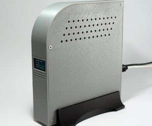
Introduction: Air Quality Monitoring Using Particle Photon
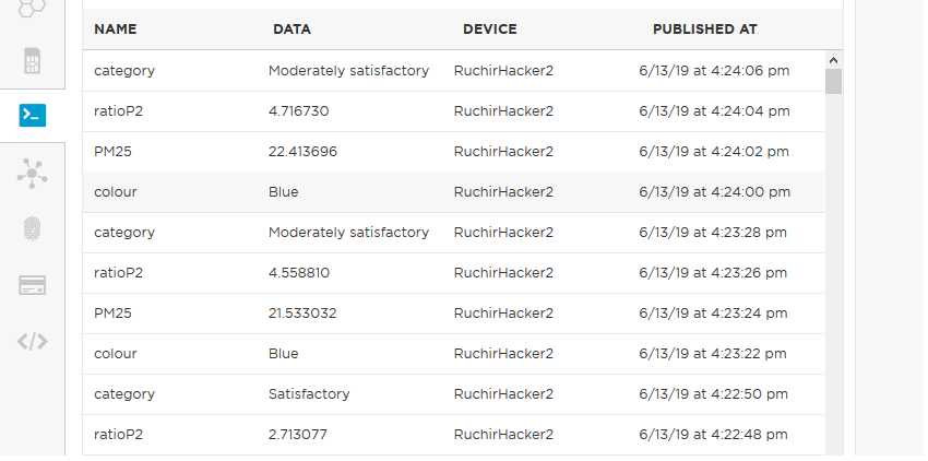
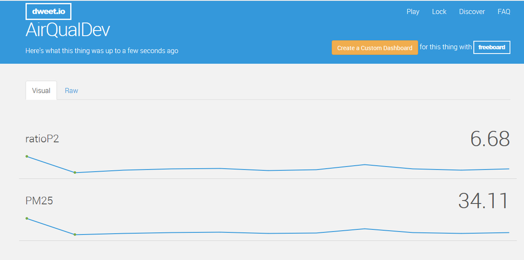
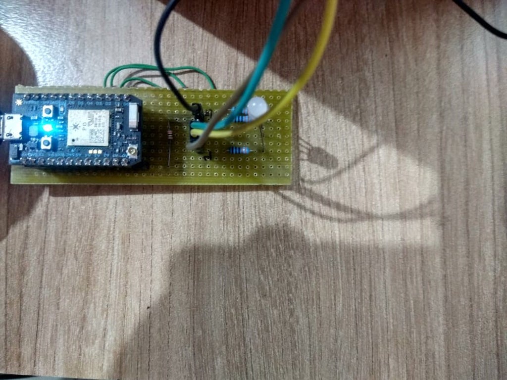
In this project PPD42NJ particle sensor is used to measure the air quality (PM 2.5) present in the air with Particle Photon. It not only display the data on Particle console and dweet.io but also indicate the air quality using RGB LED by changing its color.

Step 1: Components
Hardware
- Particle Photon ==> $ 19
- Seeed PPD42NJ dust sensor ==> $7.20
- RGB anode / cathode LED ==> $ 1
- 10k Resistor ==> $ 0.04
- 3 x 220 Ω Resistor ==> 0.06
Software
- Particle Web IDE
- dweet.io
Total price is around $ 28
Step 2: About PM
What is PM level
Particulate matter (PM) in the atmospheric air or in any other gas cannot be expressed in terms of ppmv, volume percent or mole percent. PM is expressed as mg/m^3 or μg/m^3 of air or other gas at a specified temperature and pressure.
Note:- One volume percent = 10, 000 ppmv (parts per million by volume) with a million being defined as 10^6.
Care must be taken with the concentrations expressed as parts per billion by volume (ppbv) to differentiate between the British billion which is 10^12 and the USA billion which is 10^9.
Particulate matter is the sum of all solid and liquid particles suspended in air many of which are hazardous. This complex mixture includes both organic and inorganic particles.
Based on size, particulate matter is often divided into two groups.
1. Coarse particles (PM 10-2.5) such as those found near roadways and dusty industries range in diameter from 2.5 to 10 micrometers (or microns). The existing coarse particle standard (known as PM 10) includes all particles less than 10 microns in size.
2. "Fine particles" (or PM 2.5) are those found in smoke and haze have diameters less than 2.5 microns. PM 2.5 is referred to as "primary" if it is directly emitted into the air as solid or liquid particles, and is called "secondary" if it is formed by chemical reactions of gases in the atmosphere.
Which of PM2.5 and PM10 is more harmful?
The smaller particles or PM2.5 are lighter and go deeper into the lungs and cause greater damage longer term. They also stay in the air longer and travel farther. PM10 (big) particles can stay in the air for minutes or hours while PM2.5 (small) particles can stay in the air for days or weeks.
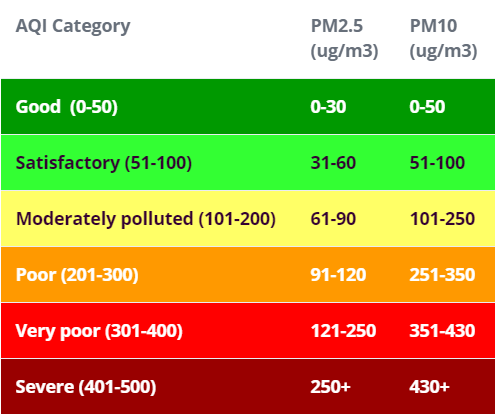
Note:- PM2.5 or PM10 data on online websites is represented as AQI or ug/m3. If the PM2.5 value is 100, then if it is represented as AQI then it will fall in the 'Satisfactory' category but if it is represented as ug/m3 then it will fall under the 'Poor' category.
Step 3: PPD42NJ Dust Sensor
Based on the light scattering method, it detects airborne particles continuously. Pulse output that corresponds to concentration per unit volume of particles can be obtained with using an original detection method based on light scattered principle similar to the particle counter.
Front side
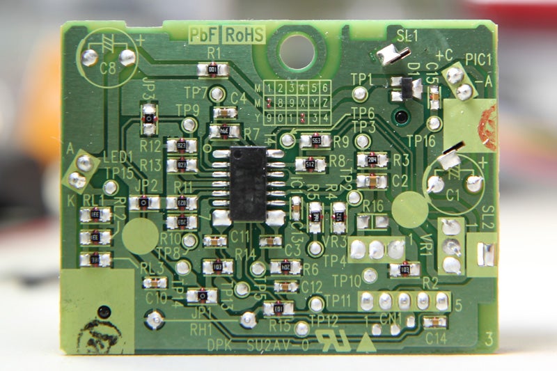
On the front, it has 2 pots labelled VR1 and VR3 that have been already factory-calibrated. The IR detector is covered under the metal can. Interestingly there’s a slot by the side labelled SL2 which is unused.

 Back side
The circuit consists largely of passives and an op-amp. RH1 is the resistor heater which, in theory, could be removed to save power if there was some other method of air circulation.
Pin Description
Sensor Placement
There are several points that should be observed when deciding how the sensor is placed.
- The sensor must be placed in a vertical orientation. Any other orientation would not achieve the desired airflow.
- The sensor should be kept in a dark condition.
- Soft cushioning material to seal the gap between sensor and housing is necessary.
Seal the gap using foil paper as shown below

Talking about sensor output
The sensor output is normally high, but goes low in proportion to the PM concentration, hence by measuring what they call Low Pulse Occupancy (LPO), the PM concentration can be determined. This LPO is recommended to be measured over a unit time of 30 seconds.
Step 4: RGB LED
There are two kinds of RGB LEDs:
- Common anode LED
In a common anode RGB LED, the three LEDs share a positive connection (anode).
- Common cathode LED
In a common cathode RGB LED, all three LEDs share a negative connection (cathode).
RGB LED Pins

Step 5: Particle Photon
Photon is a popular IOT board.The board houses STM32F205 120Mhz ARM Cortex M3 microcontroller and has 1 MB flash memory, 128 Kb RAM and 18 mixed signal general purpose input output (GPIO) pins with advanced peripherals. The module has on-board Cypress BCM43362 Wi-Fi chip for Wi-Fi connectivity and Single band 2.4GHz IEEE 802.11b/g/n for Bluetooth. The board comes equipped with 2 SPI, one I2S, one I2C, one CAN and one USB interface. It should be noted that 3V3 is a filtered output used for analog sensors. This pin is the output of the on-board regulator and is internally connected to the VDD of the Wi-Fi module. When powering the Photon via VIN or the USB port, this pin will output a voltage of 3.3VDC. This pin can also be used to power the Photon directly (max input 3.3VDC). When used as an output, the max load on 3V3 is 100mA. The PWM signals have a resolution of 8-bit and run on a frequency of 500 Hz.
Pin Diagram

Pin Description

Step 6: Dweet.io
dweet.io enables your machine and sensor data to become easily accessible through a web based
RESTful API, allowing you to quickly make apps or simply share data.
1. Go to dweet.io
2. Go to dweets section and create dweet for a thing

3. You will see page like this. Enter a unique name of a thing. This name will be used in Particle photon.

Now, we are done with dweet.io setup
Step 7: Particle Web IDE
For writing the program code for any Photon, developer needs to create an account on Particle website and register the Photon board with his user account. The program code then can be written on Web IDE at the Particle's website and transferred to a registered photon over the internet. If the selected Particle board, Photon here, is switched on and connected to cloud service of the Particle, the code is burnt to the selected board over the air via internet connection and the board starts operating according to the transferred code. For controlling board over the internet, a web page is designed which uses Ajax and JQuery to send data to the board using HTTP POST method. The web page identifies the board by a device ID and connects to the Particle's Cloud Service through an access token.
How to connect photon with Internet
1. Power your device
- Plug the USB cable into your power source.
- As soon as it is plugged in, the RGB LED on your device should begin blinking blue.If your device is not blinking blue, hold down the SETUP button.If your device is not blinking at all, or if the LED is burning a dull orange color, it may not be getting enough power. Try changing your power source or USB cable.
2. Connect your Photon to the Internet
There are two ways either you use web application or mobile app
a. Using web application
- Step 1 Go to particle.io
- Step 2 Click on setup a Photon
- Step 3 After clicking on NEXT, you should be presented with a file (photonsetup.html)
- Step 4 Open the file.
- Step 5 After opening the file connect your PC to the Photon, by connecting to the network named PHOTON.
- Step 6 Configure your Wi-Fi credentials.
Note: If you mistype your credentials, the Photon will blink dark blue or green. You have to go through the process again (by refreshing the page or clicking on the retry process part)
- Step 7 Rename your device. You will also see a confirmation if the device was claimed or not.
b. Using smartphone
- Open the app on your phone. Log in or sign up for an account with Particle if you don't have one.
- After login, press the plus icon and select the device you'd like to add. Then follow the instructions on the screen to connect your device to Wi-Fi. If this is your Photon's first time connecting, it will blink purple for a few minutes as it downloads updates. It may take 6-12 minutes for the updates to complete, depending on your internet connection, with the Photon restarting a few times in the process. Do not restart or unplug your Photon during this time.
Once you have connected your device, it has learned that network. Your device can store up to five networks. To add a new network after your initial setup, you'd put your device into Listening Mode again and proceed as above. If you feel like your device has too many networks on it, you can wipe your device's memory of any Wi-Fi networks it has learned. You can do so by continuing to hold the setup button for 10 seconds until the RGB LED flashes blue quickly, signaling that all profiles have been deleted.
Modes
- Cyan, your Photon is connected to the Internet.
- Magenta, it is currently loading an app or updating its firmware. This state is triggered by a firmware update or by flashing code from the Web IDE or Desktop IDE. You might see this mode when you connect your Photon to the cloud for the first time.
- Green, it is trying to connect to the internet.
- White, the Wi-Fi module is off.
Web IDE
Particle Build is an Integrated Development Environment, or IDE that means that you can do software development in an easy-to-use application, which just so happens to run in your web browser.
- To open build, login to your particle account and then click on Web IDE as shown in image.

Once you clicked you will see console like this.

To create a new create app, click on create new app.

To verify the program. Click on verify.

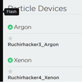
To upload the code, click on flash but before doing that select a device.If you have more than one device you have to make sure that you have selected which of your devices to flash code to. Click on the "Devices" icon at the bottom left side of the navigation pane, then when you hover over device name the star will appear on the left. Click on it to set the device you had like to update (it won't be visible if you have only one device). Once you have selected a device, the star associated with it will turn yellow. (If you only have one device, there is no need to select it, you can continue.

Step 8: Connections
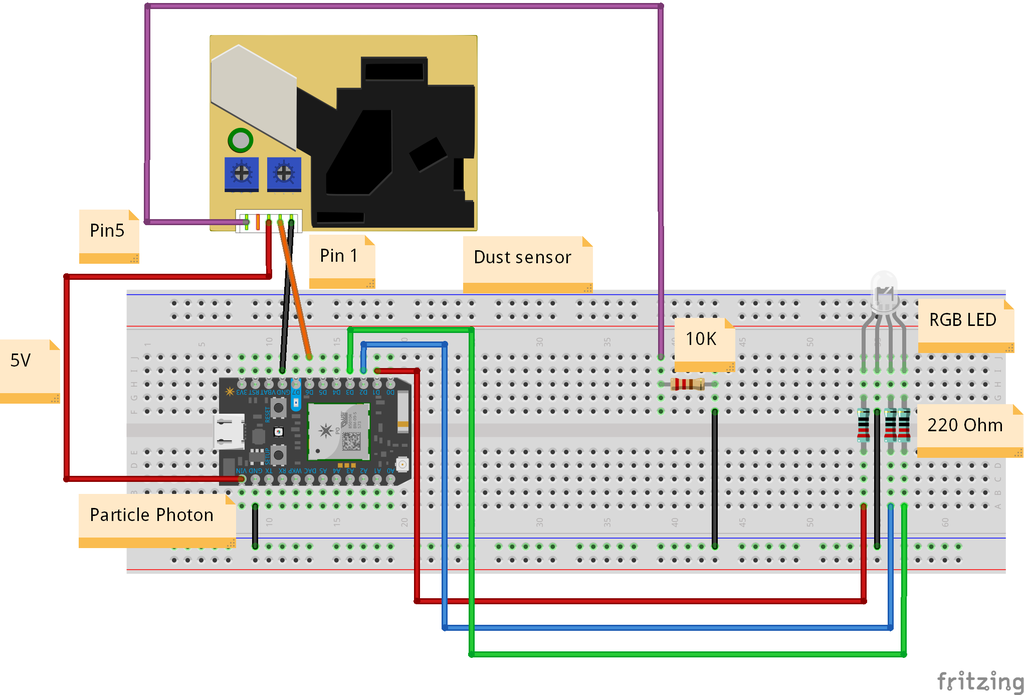
Particle Photon ==> PPD42NJ sensor (placed in vertical direction)
GND ==> Pin1(GND)
D6 ==> Pin2 (Output)
Vin ==>Pin3(5V)
GND ==> 10k resistor ==> Pin5 (Input)
Particle Photon ==> RGB LED
D1 ==> R
D2 ==> G
D3 ==> B
GND ==> Common Cathode (-)
Step 9: Program
Attachments
Step 10: Result
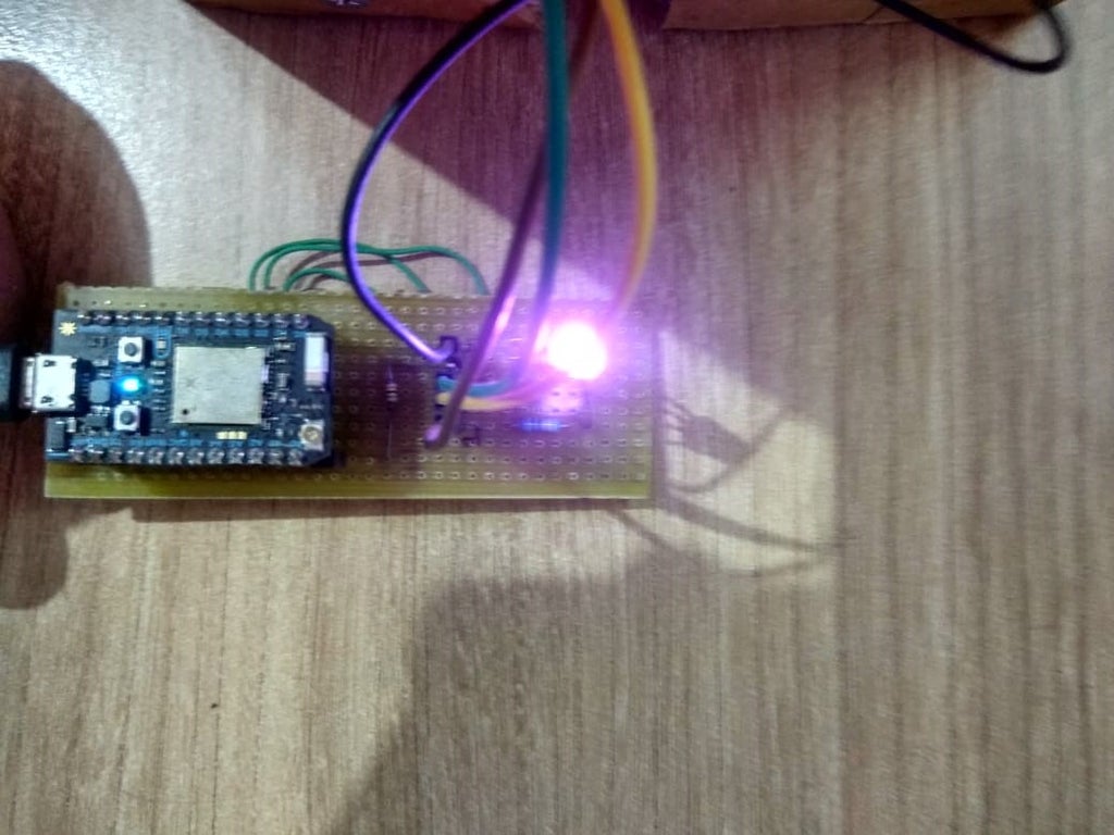
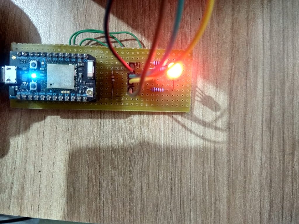
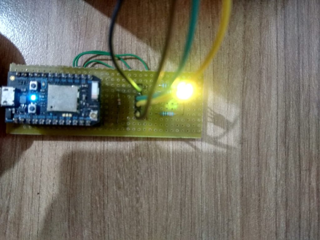
Step 11: How to Make PCB in Eagle
What is PCB
PCB is a printed circuit board which electrically connects a set of electronic components by using copper tracks on a non-conductive board. In PCB, all components are connected without wires, all components are connected internally, so it will reduce the complexity of the overall circuit design.
Types of PCB
1.Single-sided PCB
2.Double-sided PCB
3. Multi-layered PCB
In this, I am only talking about Single-sided PCB
Single-sided PCB
A single layer PCB is also known as single-sided PCB. This type of PCB is simple and most used PCB because these PCBs are easy to design and manufacture. One side of this PCB is coated with a layer of any conducting material. Copper is used as conducting material because it has a very good conducting characteristic. A layer of solder mask is used to protect PCB against oxidation followed by silkscreen to mark out all of the components on the PCB. In this type of PCB, only one side of the PCB is used to connect different types of components.
Different Parts of PCB
1. Layers
Top and bottom layer: In the Top layer of PCB, all SMD components are used. Generally, this layer is Red-colored. In the bottom layer of PCB, all components are soldered through the hole and lead of components is known as the bottom layer of PCB. In this DIP components are used and the layer is blue.

Copper tracks
It's generally a conducting path between components in the circuits for an electrical contact or a track is a conductive path that is used to connect 2 points in the PCB. For instance, connecting 2 pads or connecting a pad and a via or between vias. The tracks can have different widths depending on the currents that flow through them.
We Use Copper because it is highly conductive. This means that it can easily transmit signals without losing electricity along the way. In the most common configuration, an ounce of copper can be turned into 35 micrometres about 1.4 thousandths of an inch thick, which can cover an entire square foot of the PCB substrate.
Pads
A pad is a small surface of copper in a printed circuit board that allows soldering the component to the board or we can say points on the circuit board where the terminals of the components are soldered.
There are 2 types of pads; thru-hole and SMD (surface mount).
- Thru-hole pads are intended for introducing the pins of the components, so they can be soldered from the opposite side from which the component was inserted.
- The SMD pads are intended for surface mount devices, or in other words, for soldering the component on the same surface where it was placed.
Shapes of Pads
- Circular
- Oval
- Square

Soldermask
For mounting the electrical components on the printed circuit boards, an assembly process is required. This process can be done by hand or through specialized machinery. The assembly process requires the use of solder to place the components on the board. For avoiding or to prevent the solder to accidentally short-circuit two tracks from different nets, PCB manufacturers apply a varnish called soldermask on both surfaces of the board. The most common colour of the soldermask used in printed circuit boards is green. This insulating layer is used to prevent accidental contact of pads with other conductive material on PCB.
Silkscreen
Silk-screening (Overlay) is the process where the manufacturer prints information on the soldermask conducive to facilitate the processes of assembly, verification, and debugging. Generally, the silkscreen is printed for indicating test points as well as the position, orientation, and reference of the electronic components that are part of the circuit. Silkscreen can be printed on both surfaces of the board.
Via
A via is a plated hole that allows the current to pass through the board. It is used in the multilayer PCB to connect to more layers.
Types of Via
- Thru-hole Vias or Full Stack Vias
When an interconnect must be made from a component that is located on the top layer of the printed circuit board with another that is located at the bottom layer. For conducting the current from the top layer to the bottom layer, a via is used for each track.
Green ==> Top and bottom soldermasks
Red ==> Top layer ( conductive )
Violet ==> Second layer. In this case, this layer is used as a power plane ( i.e. Vcc or Gnd )
Yellow ==> Third layer. In this case, this layer is used as a power plane ( i.e. Vcc or Gnd )
Blue ==> Bottom Layer ( conductive )

2. Blind vias
blind vias are used, which allows a connection to be made from an external layer to an internal layer with minimum via height. A blind via starts on an external layer and ends on an internal layer, that's why it has the prefix "blind". In multilayer system designs where there are many integrated circuits, power planes ( Vcc or GND) are used to avoid excessive routing for power rails.
To know if a certain via is blind, you can put the PCB against a source of light and see if you can see the light coming from the source through the via. If you can see the light, then the via is thru-hole, otherwise, the via is blind.
It is very useful to use these kinds of vias in printed circuit board design when you don't have too much space for placing components and routing. You can put components on both sides and maximize the space. If the vias were thru-hole instead of blind, there would be some extra space used by the vias on both sides.

3. Buried Vias
These vias are similar to the blind ones, with the difference that they begin and end on an inner layer.

ERC
After creating the schematic and annotating circuit, it is necessary to check whether the circuit has any electrical errors such as, if Nets are not connected properly, the input is not connected to the input pin, Vcc and GND shorted anywhere in the circuit, or any pin electrical type not selected properly, etc. All these are electrical error types. If we have made any such mistake in the schematic, and if we are not performing any ERC, then after completing the PCB we cannot get the desired result from the circuit.
Design rule check
DRC Detail
How to make PCB in Eagle
Make a schematic diagram
1. To make a schematic go to File ==> new ==> Schematic You will see a page like this

As there are no Particle parts so we have to add Particle devices libraries.
Next, after downloading it move it to the folder C:\Users\.....\Documents\EAGLE\libraries

In Eagle open Schematics go to Library ==> open library manager

you will see a page like this, go to option Available and browse to the library particledevices.lbr

After opening it click on use

Now, we can see particle devices.
Next step is to make a schematic for that we use add part as shown in figure

When you click on add part you will see a page like this

The components we needed are Particle photon, headers, resistors, GND, Vcc. Search components in add parts
- For a resistor, there are two types US and EU. Here I am using a European one
- For header search header and you will see lots of headers choose according to yours.
- For ground search gnd
- For VCC search vcc
- For Particle Photon search it
Once components are selected next step is to join it together for that you can use line or nets or both.


Join it as shown in the image below

Next step is giving name and value.


For giving names select name and then click on the component to which you wanna give a name.
For giving values select value and then click on the component to which we want to give a name.
After that check ERC

Once checked we are done with Schematic. Next step is to switch to boards from schematics

When you shift to boards you will see all the components at the left side of the board so you have to move it to the PCB board. For that click on the group and select all the components and use the move tool to move it.


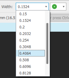
After that assemble all the components as per your convenience. For joining the components use route airwire make sure you will use the bottom layer, the grid will be in mm and route airwire width 0.4064



After joining all the components Use mirror tool to generate an image of values and names.


For using mirror first select mirror tool and then values, names.
Next, save the board with any name, check DRC to check errors. If no error we are good to go ahead.
To see a preview of the board go to manufacturing.
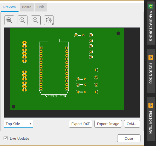

Now we are done with the board part.
Next step is to print the ckt on glossy paper. For that click on print, you will see a page as shown below.

- Select black in option, if you are using multiple layers then you also have to select mirror.
- Select scale factor 1.042 After that save it to pdf or print it.
After printing the ckt,
1. Remove the oxidation layer using sandpaper (400) use a light hand.

2. Clean it using isopropanol or propan-2-ol or if you want you can use thinner also.
3. Place the printed ckt on FR4 sheet using paper tape.
4. Heat it using heating iron (5 -10 minutes) so that ckt will print on FR4 sheet. Soak board in water for 2-3 minutes. After that remove the tape and paper.

5. Place it in ferric chloride solution for 10 minutes to remove access copper then wash it with water.


6. Remove the layer using sandpaper(400) or Acetone.


Participated in the
Sensors Contest


