Introduction: Arduino Cell Phone 4G Signal Booster / Repeater Part 1


Living on an island in the middle of nowhere, mobile/cell phone reception can be rather intermittent and it seems that there is currently no reliable open source gadget that could help me solve this problem on my kind of budget.
I do have the option of using 'cable phone' but being of a general 'Pirate' disposition I thought it would be a better idea to do all my phone calls, emails and data transactions by cell phone and save a whole bunch of dollars by not having to pay for land based line rental and broadband etc. Doing everything through my phone is a lot cheaper and still plenty quick enough to watch films and videos without any buffering.
I actually tried buying an off the shelf repeater but it completely jammed my phone up and I started to get worried that it was going to damage it, so instead I opened it up to see how it worked - maybe I could repair it? Unfortunately none of the components could be identified and furthermore, it looked like it had been severely 'messed about with' at the factory. The soldering looked very poor and a large piece of metal swarf fell out of the opened case :(
I did search on the Interweb for tutorials and information on how to build this kind of device but, unfortunately, there was only one single piece of information:
https://www.instructables.com/id/4G-LTE-Home-Repeater-With-LimeSDR/
I did actually re-create this instructable and, after 6 weeks constant toil, got it to work but decided to create a separate, simpler version, which is this one documented here!
With absolutely no previous radio frequency (RF) experience, the challenge was to learn how a repeater works by playing around with a software defined radio (SDR) and then build one from scratch with the necessary hardware filters, amplifiers and controls.
The 'RepeaterDuino' / 'RepeatDuino' / 'RFBoostDuino' / 'RFRepeatDuino' / 'OpenRFRepeater' / 'PeoplesRepeater' / 'PirateRepeater' is born!
Step 1: How It Works


The cell phone base station signals are constantly being transmitted from one or more masts owned by the phone company. In my case, I can only reliably receive the 4G signal if I stand on a roof or raise my phone up a pole like a flag so an external antenna mounted 20 feet up a pole is necessary.
The external antenna receives the good quality signal and sends it down a shielded cable to a filter which very accurately stops everything except a very small slice of frequencies. For my phone, these frequencies are centered around 806 MHz and have a spread, or bandwidth, of 30 MHz.
The signal then goes into a LNA (Low Noise Amplifier) which does a fair bit of amplification at low power and .... as it says on the tin, very low noise aberrations. It's much more efficient to 'cascade' the amplifiers rather than try and do everything with one device.
Next is the Variable Gain Amplifier, or VGA, which does most of the grunt work and has the ability to be controlled by a microprocessor by means of very simple SPI code. The gain needs to be controlled as sometimes the base station signal can be quite strong and we don't want to damage our phone or create a feedback loop between the two antennae. The antennae have to be spaced well apart or separated by thick walls or metal sheeting.
Simultaneously, the signal comes out of the BPF and routes into an RSSI (Received Signal Strength Indicator) which provides an analogue signal ie a DC voltage to the micro controller, which can turn down the VGA if the signal is too strong. At the moment, control of the VGA is manual by means of a slide potentiometer.
The amplified signal goes out of the VGA into a plate antenna which is located inside the building and transmits the signal to the cell phone.
Step 2: Video Demonstarion
This video above shows all the main components of the repeater, which is demonstrated using my own phone and a spectrum analyser, which has a small 'whip' antenna located right next to the plate antenna. The spectrum analyser is actually a Software Defined Radio (SDR) which can be bought for as little as $10!
Step 3: Building the Band Pass Filters


Legal:
Please check your local laws / telecoms regulations before embarking on this project.
Tools and Components Required:
- Small electric oven
- Stop watch
- K type thermometer
- PCB board (see file attached - it opens with 'Design Spark' software)
- Lead free solder paste
- CTS USD020A duplexer
- UFL sockets - male.
- UFL cable - female to female
Just before we start, we are only using one side of the duplexer and the other side is available if the project needs to be expanded at a later date.
Apply small dabs of solder paste to the PCB paying special attention to the actual terminals of the filter. Carefully place the filter and UFL sockets on the PCB and apply a small amount of downward pressure.
Put the PCB in the oven and follow the manufacturer's temperature profile (see attached PDF) by monitoring with a stopwatch and thermometer. The profile is different to most other SMT components as the filters are large blocks of ceramic that take longer to get hot.
Notice that the filters are machined with tiny scour marks - these are tuning marks made at the factory to get super accurate results.
The antenna socket is in the middle and the 806 MHz socket, when looking at the first photo, is on the right hand side.


Step 4: Low Noise Amplifier Module


Components:
- U1 n/a 2-Stage Bypass LNA Qorvo QPL9065
- R1, 2, 3, 5, 7 0 Ω RES, 0402, +/-5%, 1/16W Various
- R10 39K RES, 0402, +/-5%, 1/16W Various
- C1 0.5 pF CAP, 0402, +/-0.1pF, 50V, C0G Murata GJM1555C1HR50BB01D
- R9 5.1 Ω RES, 0402, +/-5%, 1/16W various
- L1 1.5 nH IND, 0402, +/-0.1nH, 1000mA Murata LQP15MN1N5B02D
- L4 6.8 nH IND, 0402, +/-2%, 700mA Murata LQG15HS6N8J02
- C2, 3, 4, 5, 7 100 pF CAP, 0402, +/-5%, 50V Various
- C6, 8 0.1 uF CAP, 0402, 20%, 16V, Y5V Various
- C9 10 pF CAP, 0201, 2%, 50V Murata GRM0335C1H100GA01
- C12 4.7 uF CAP, 0603, 20%, 10V, Y5V Various
- C10, 11 10 pF CAP, 0402, 2%, 50V various
- L2 2.2 nH IND, 0402, +/-0.2nH, 1000mA Murata LQW15AN2N2C10
- L5 18 nH IND, 0603, 5% Coilcraft 0603CS-18NXJL
- LNA Amp PCB and paste mask stencil - see attached file.
Use the solder mask stencil to apply solder paste and reflow in an electric oven. with a standard reflow profile.
Rather than actually build the whole PCB from scratch, the Qorvo evaluation board is a good option: Evaluation Board.
Step 5: Variable Gain Amplifier


Component: TQM879028-PCB2140
I made my life a lot easier by, in this case, purchasing this device as an evaluation board: Evaluation board. The circuit comes with a detachable USB adaptor and software so that in can be controlled by a PC for testing. The device is supplied by a company called Qorvo and their customer service is excellent!
In this project the device is wired up to an Arduino Uno and controlled by 3 wire SPI. Looking at the photo:
- The black wire, bottom left goes to ground.
- The red wire, top left, goes to 5V.
- The red wire, top right, goes to 5V.
- The white wire, pin 5 from the left, front, goes to Arduino Uno pin13 (Clock).
- The blue wire, pin 4 from the left, rear, goes to Uno pin 10 (Chip Select)
- The grey wire, pin 5, rear, goes to Uno pin 11 (MOSI).
The code for controlling the device is very simple:
#include <SPI.h>
const int slaveSelectPin = 10;
void setup()
{
  pinMode(slaveSelectPin, OUTPUT);
  SPI.begin();
}
void loop()
{
// Sets the VGA to 40 out of a max of 63:
      digitalPotWrite(40);
      delay(1000);
}
void digitalPotWrite(int rabbits)
{
  digitalWrite(slaveSelectPin, LOW);
  SPI.transfer(rabbits);
  digitalWrite(slaveSelectPin, HIGH);
}
Step 6: RSSI

Components:
- AD8318
- Male SMA, female UFL cable
This component can be bought cheaply on Ebay HERE. It plugs into the input of the LNA board (or the output of the filter) via a male SMA, female UFL cable.
I hacked the output by attaching a green and red wire to the PCB although it actually only needs the red wire, which goes to an analogue input (0) on the Uno. The code for reading the signal is very simple:
int rssiValue = analogRead(0);
Step 7: TFT Screen


Component:2.2" 18-bit color TFT LCD display with microSD card breakout
Apart from the TFT screen, there is a 10 x 3 0.1" strip of PCB for allowing multiple connections on the SPI bus.
The screen wiring is fairly obvious except that:
- D/C connects to pin 9 on the Uno.
- CS connects to pin 7.
- MOSI to pin 11.
- SCK to pin 13.
The code requires the following:
#include "SPI.h"
#include "Adafruit_GFX.h"
#include "Adafruit_ILI9341.h"

// For the Adafruit shield, these are the default.
#define TFT_DC 9
#define TFT_CS 7
#define TFT_RST  2  // Reset line for TFT (or connect to +5V)
#define TFT_MOSI 11
#define TFT_MISO 12
#define TFT_CLK 13
Step 8: Antennae

The outside antenna is HERE and is a Quad Band Cellular Antenna with a male SMA connector. It connects to the middle UFL socket on the filter PCB.
The inside antenna is a plate type as shown in the photo (protective case removed) and also requires a male SMA. This connects to the output of the VGA amp.
IMPORTANT: The two antennae must be isolated from one another by thick stone walls or metal sheeting and the gain on the VGA should not be increased to such an extent that you get feedback between the device signal input and output. If a strong signal is suddenly supplied to the input of the device it may damage cell phones in the near vicinity.
Step 9: Main PCB


Components: Alps RSA0N Series Slide Potentiometer with a 18.5 x 1.5 mm Dia. Shaft, 10kΩ, ±20%, 0.5W, Through Hole
This board is actually from another one of my projects, but is perfect for a base for this one (See Stepper Motor PCB file attached). The Arduino Uno sits under the PCB at the top left corner with the appropriate headers. The slider potentiometer sits on the far right.
Attachments
Step 10: Arduino Uno Code
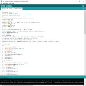
There's nothing unusual about the Arduino code, except that reading the VGA via SPI must be terminated with 'SPI.end();' on each read.
Code:
#include "SPI.h"
#include "Adafruit_GFX.h"
#include "Adafruit_ILI9341.h"

// For the Adafruit shield, these are the default.
#define TFT_DC 9
#define TFT_CS 7
#define TFT_RST  2  // Reset line for TFT (or connect to +5V)
#define TFT_MOSI 11
#define TFT_MISO 12
#define TFT_CLK 13

const int slaveSelectPin = 10; // LE for the VGA.
int sensorPin = A3;    // select the input pin for the potentiometer
float sensorValue = 1.00;
int rabbits;
int rssiValue = 0;
// Use hardware SPI (on Uno, #13, #12, #11) and the above for CS/DC
//Adafruit_ILI9341 tft = Adafruit_ILI9341(TFT_CS, TFT_DC);
// If using the breakout, change pins as desired
Adafruit_ILI9341 tft = Adafruit_ILI9341(TFT_CS, TFT_DC, TFT_MOSI, TFT_CLK, TFT_RST, TFT_MISO);

void setup()
{
  Serial.begin(9600);
  Serial.println("ILI9341 Test!");
  writePotToVGA();
  tft.begin();
  tft.setRotation(3);
  tft.fillScreen(ILI9341_BLACK);
  rectangle1();
  introText();
  staticText ();
  //delay(5000);

  // set the slaveSelectPin as an output:
  pinMode(slaveSelectPin, OUTPUT);
  // initialize SPI:
//  SPI.begin();
//  digitalPotWrite(10);
//  delay(5000);
//  digitalPotWrite(20);
 // delay(5000);
 // digitalPotWrite(30);
//  delay(5000);
 // SPI.end();
  //tft.fillScreen(ILI9341_BLACK);
}
void loop(void)
{
   rssiValue = analogRead(0);
   Serial.println(rssiValue);
   testText();
   //digitalPotWrite(40);
   delay(1000);
   writePotToVGA();
}

void writePotToVGA()
{
  sensorValue = analogRead(sensorPin);
  sensorValue = sensorValue*63/1023;
  rabbits = sensorValue;
  SPI.begin();
  digitalWrite(slaveSelectPin, LOW);
  SPI.transfer(rabbits);
  digitalWrite(slaveSelectPin, HIGH);
  SPI.end();
}
void digitalPotWrite(int rabbits)
{
  // take the SS pin low to select the chip:
  digitalWrite(slaveSelectPin, LOW);
  //  send in the address and value via SPI:
 // SPI.transfer(address);
  SPI.transfer(rabbits);
  // take the SS pin high to de-select the chip:
  digitalWrite(slaveSelectPin, HIGH);
}
unsigned long introText()
{
  tft.setRotation(3);
  rectangle2 ();
  tft.setTextColor(ILI9341_GREEN);
  tft.setTextSize(3);
  tft.setCursor(20, 20);
  tft.println("4G Repeater");
  tft.setCursor(20, 200);
  tft.println("Band 20, 806 Mhz");
}
unsigned long testText()
{
  rssiValue = analogRead(0);
  sensorValue = analogRead(sensorPin);
  sensorValue = sensorValue*63/1023;
  tft.setRotation(3);
  rectangle2 ();
  tft.setTextColor(ILI9341_GREEN);
  tft.setTextSize(3);
  tft.setCursor(250, 70);
  tft.println(sensorValue,0);
  tft.setCursor(250, 100);
  tft.println(rssiValue);

  delay (1000);
}
void rectangle2 ()
{
          tft.fillRect(220, 65, 100, 65, ILI9341_BLUE);
          // x,y,(from top left corner)w,h
}
void rectangle1 ()
{
          tft.fillRect(0, 65, 320, 65, ILI9341_RED);
          // x,y,(from top left corner)w,h
}
void staticText ()
{
  tft.setCursor(10, 70);
  tft.println("VGA gain:");
  tft.setCursor(10, 100);
  tft.println("RSSI level:");
}
Step 11: Testing the Device


Check with your cell phone network which band your phone uses for 4G eg band 20, or try and locate it with an SDR.
A cheap SDR (Software Defined Radio) - see photo - can be also used to monitor the performance of the cell phone repeater. Pay no more than $10!
Position the SDR antenna right next to the repeater's plate antenna and tune the SDR to about 806 MHz. As the slider pot is moved from left to right, an increase in brightness of the lines on the waterfall should be seen. They may even turn to yellow or even red. Adjust the gain and FFT settings in the software to get coherent results.
A phone can also be used to check the device is working, the SDR must be used in the first instance and all phones nearby should be turned off to avoid damaging them during initial testing. There are apps available for smart phones to monitor signal strength more accurately than the regular 'bar' type displays.
Step 12: Final

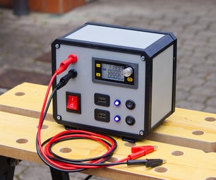
The device is big and clunky with lots of wires going all over the place but it works really well and, being bolted to one PCB, is pretty solid. It now needs some long term testing to check that none of the components break down too quickly etc. Eventually, at some time in the future, it will get reduced to one small Arduino shield with the ability to user change the filters for different 4G bands.
In terms of power and range, in it's current configuration the power is probably at about 1mA which is giving an effective range of about 3 metres. This might seem very low, but it's actually very beneficial to run at low power as it's normally under the threshold for serious transmit licensing (check your local regulations) and it's very much less likely to cause feedback with the external pole mounted antennae. The only downside is that the cell phone has to be within 3 metres of the internal antenna.
Please feel free to ask questions or make constructive criticism but be aware that I know very little about RF so may not be able to answer the more technical queries.
Thank you!
| Please |

Participated in the
Power Supply Contest

Participated in the
Invention Challenge 2017

Participated in the
Untouchable Challenge