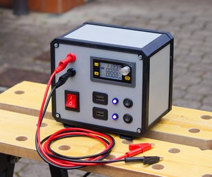
Introduction: Desk Amplifier With Audio Visualization, Binary Clock & FM Receiver


I like amplifiers and today, I will share my low power desk amplifier I made recently. The amplifier I designed has some interesting features. It has an integrated binary clock and can give time and date and it can visualize audio often called audio spectrum analyzer. You can use it as FM receiver or MP3 player. If you like my clock amplifier then follow the steps below to make your own copy.
Step 1: Good Amplifier Design Tips


Designing a noise free good quality audio circuit is really hard even for an experienced designer. So, you should follow some tips to make your design better.
Power
Loudspeaker amplifiers typically are powered directly from the main system voltage and require relatively high current. Resistance in the trace will result in voltage drops that reduce the supply voltage of the amplifier and waste power in the system. The trace resistance also causes the normal fluctuations in supply current to convert to fluctuations in voltage. To maximize performance, use short wide traces for all amplifier power supplies.
Grounding
Grounding plays the single, most significant role in determining whether the device's potential is achieved by the system. A poorly grounded system will likely have high distortion, noise, crosstalk, and RF susceptibility. Although one can question how much time should be devoted to system grounding, a carefully designed grounding scheme prevents a large number of problems from ever occurring.
The ground in any system must serve two purposes. First, it is the return path for all currents flowing to a device. Second, it is the reference voltage for both digital and analog circuits. Grounding would be a simple exercise if the voltage at all points of the ground could be the same. In reality, this is not possible. All wires and traces have a finite resistance. This means that whenever there is current flowing through the ground, there will be a corresponding voltage drop. Any loop of wire also forms an inductor. This means that whenever current flows from the battery to a load, and back to the battery, the current path has some inductance. The inductance increases the ground impedance at high frequencies.
While designing the best ground system for a particular application is no simple task, some general guidelines do apply to all systems.
- Establish a Continuous Ground Plane for Digital Circuits: Digital current in the ground plane tends to follow the same route that the original signal took. This path creates the smallest loop area for the current, thus minimizing antenna effects and inductance. The best way to ensure that all digital signal traces have a corresponding ground path is to establish a continuous ground plane on the layer immediately adjacent to the signal layer. This layer should cover the same area as the digital signal trace and have as few interruptions in its continuity as possible. All interruptions in the ground plane, including vias, cause the ground current to flow in a larger loop than is ideal, thereby increasing radiation and noise.
- Keep Ground Currents Separate: The ground currents for digital and analog circuits must be separated to prevent digital currents from adding noise to the analog circuits. The best way to accomplish this is through correct component placement. If all the analog and digital circuits are placed on separate parts of the PCB , the ground currents will naturally be isolated. For this to work well, the analog section must contain only analog circuits on all layers of the PCB.
- Use the Star Grounding Technique for Analog Circuits: Audio power amplifiers tend to draw relatively large currents that can adversely affect both their own and other ground references in the system. To prevent this problem, provide dedicated return paths for bridged-amplifier power grounds and headphone-jack ground returns. Isolation allows these currents to flow back to the battery without affecting the voltage of other parts of the ground plane. Remember that these dedicated return paths should not be routed under digital signal traces because they could block the digital return currents.
- Maximize the Effectiveness of Bypass Capacitors: Nearly all devices require bypass capacitors to provide instantaneous current. To minimize the inductance between the capacitor and the device supply pin, locate these capacitors as close as possible to the supply pin which they are bypassing. Any inductance reduces the effectiveness of the bypass capacitor. Similarly, the capacitor must be provided a low-impedance connection to ground to minimize the capacitor's high-frequency impedance. Directly connect the ground side of the capacitor to the ground plane, rather than routing it through a trace.
- Flood All Unused PCB Area with Ground: Whenever two pieces of copper run near each other, a small capacitive coupling is formed between them. By running ground flood near signal traces, unwanted high-frequency energy in the signal lines can be shunted to ground through the capacitive coupling.
Try to keep power supplies, transformer and noisy digital circuits away from your audio circuitry. Use a separate ground connection for audio circuit and it is good not to use ground planes for audio circuitry. The ground (GND) connection of audio amplifier is very important compare with ground of other transistors, IC etc, if there is ground noise between the two then the amplifier is going to output it.
Consider powering important IC's and anything sensitive using a 100R resistor between them and +V. Include a decent sized (e.g. 220uF) elect capacitor on the IC side of the resistor. If IC will pull a lot of power then ensure resistor can handle it (select a high enough wattage and provide PCB copper heat sinking if necessary) and bear in mind there will be voltage drop across the resistor.
For transformer based designs you want the rectifier capacitors to be as near to the rectifier pins as possible, and connected via their own thick tracks due to the large charging currents at the very peek of the rectified sin wave. As the output voltage of the rectifier exceeds the decaying voltage of the capacitor, impulse noise is produced in the charging circuit which can get transferred into the audio circuit if they share the same piece of copper in either of the power lines. You can't get rid of the pulse charging current so its much better to keep the capacitor local to the bridge rectifier to minimise these high current pulses of energy. If a audio amplifier is near the rectifier then don't locate a large capacitor next to the amp to avoid this capacitor causing this problem, but if there is a bit of distance then its fine to give the amplifier is own capacitor as it gets float charged from the power supply and ends up having a relatively high impedance due to the length of the copper.
Locate and voltage regulators which are used by the audio circuitry near to rectifiers / PSU input and connect with their own connections also.
Signals
Where possible avoid in and out audio signals to and from IC's running in parallel on the PCB as this can cause oscillations which feed from output back to input. Remember just 5mV can cause plenty of hum!
Keep digital ground planes away from audio GND and audio circuitry generally. Hum can be introduced into audio simply from tracks being too near digital planes.
When interfacing to other equipment, if powering some other board that includes audio circuitry (going to give or receive an audio signal) ensure there is only 1 point at which GND connects between the 2 boards and this should ideally be at the audio analog signal connection point.
For signal IO connections to other devices / the outside world its a good ideal to use a 100R resistor between the circuits GND and the outside world GND for everything (including digital parts of the circuit) to stop ground loops being created.
Capacitors
Use them wherever you want to isolate sections from each other. Values to use:- 220nF is typical, 100nF is fine if you want to reduce size / cost, best not to go below 100nF.
Do not use ceramic capacitors. The reason is that ceramic capacitors will give a piezoelectric effect to an AC signal which causes noise. Use a Poly of some type – Polypropylene is best but any will do. True audio heads also say don't use electrolytics in-line but many designers do without issue – this is likely for high purity applications not general standard audio design.
Do not use tantalum capacitors anywhere within audio signal paths (some designers may disagree but they can cause horrible problems)
A generally accepted substitute for polycarbonate is PPS (Polyphenylene Sulphide).
High quality polycarbonate film and polystyrene film and teflon capacitors and NPO/COG ceramic capacitors have very low voltage coeffficients of capacitance and hence very low distortion and the results are very clear using spectrum analyzers as well as ears.
Avoid the high-K ceramic dielectric ones, they have a high voltage coefficient which I guess could lead to some distortion if they were used in a tone control stage.
Component Placement
The first step of any PCB design is choosing where to place the components. This task is called "floor planning." Careful component placement can ease signal routing and ground partitioning. It minimizes noise pickup and the board area required.
The component placement within the analog section must be selected. Components should be placed to minimize the distance that audio signals travel. Locate the audio amplifier as close to the headphone jack and loudspeaker as possible. This positioning will minimize EMI radiation from Class D speaker amplifiers, and minimize the noise susceptibility of low-amplitude headphone signals. Place the devices supplying the analog audio as close to the amplifier as possible to minimize noise pickup on the amplifier inputs. All input signal traces will act as antennas to RF signals, but shortening the traces helps reduce the antenna efficiency for frequencies typically of concern.
Step 2: You Need...


1. TEA2025B Audio Amplifier IC (ebay.com)
2. 6 pcs 100uF Electrolytic Capacitor (ebay.com)
3. 2 pcs 470uF Electrolytic Capacitor (ebay.com)
4. 2 pcs 0.22uF Capacitor
5. 2 pcs 0.15uF Ceramic Capacitor
6. Dual Volume Control Potentiometer (50 - 100K) (ebay.com)
7. 2 pcs 4 ohm 2.5W Speaker
8. MP3 + FM Receiver Module (ebay.com)
9. LED Matrix With Driver IC (Adafruit.com)
10. Vero Board & Some wires.
11. Arduino UNO (Adafruit.com)
12. DS1307 RTC Module (Adafruit.com)
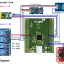
Step 3: Making the Amplifier Circuit


According the attached circuit diagram solder the entire components into the PCB. Use accurate value for the capacitors. Be careful about the polarity of the electrolytic capacitors. Try to keep all the capacitor as near as possible to the IC to minimize the noise. Directly solder IC without using IC base. Make sure you cut the traces between the two sides of the amplifier IC. All solder joint should be perfect. This is an audio amplifier circuit, so be professional about the soldering connection especially about ground (GND).
Step 4: Testing the Circuit With Speaker


After completing all the connection and soldering, connect two 4 ohm 2.5W speaker to the amplifier circuit. Connect a audio source to the circuit and power it up. If everything goes well you will here the noise free sound.
I used TEA2025B audio amplifier IC for audio amplification. It is a nice audio amplifier chip which operated in a wide voltage range (3 V to 9 V). So, you can test it with any voltage within the range. I am using 9V adapter and is working fine. The IC can operate dual or bridge connection mode. For more details about the amplifier chip please check the datasheet.
Attachments

Step 5: Preparing Dot Matrix Front Panel


For the visualization of audio signal and displaying date and time I set a dot matrix display in the front side of the amplifier box. To do the job nicely I used rotary tool to cut the frame according to the size of the matrix. If your display has no integrated driver chip use one separately. I prefer Bi-color matrix from Adafruit. After selecting perfect matrix display adjust the display to the base with hot glue.
We will connect it to Arduino board later. The bi-color display from Adafruit use i2c protocol to communicate with microcontroller. So, we will connect SCL and SDA pin of the driver IC to the Arduino board.
Step 6: Programming With Arduino


Connect Adafruit Smart Bi-color dot matrix display as:
- Connect the Arduino 5V pin to the LED matrix + pin.
- Connect Arduino GND pin to both the mic amp GND pin and the LED matrix – pin.
- You can use a breadboard power rail, or the Arduino has multiple GND pins available.Connect Arduino analog pin 0 to the audio signal pin.
- Connect Arduino pins SDA and SCL to the matrix backpack D (data) and C (clock) pins, respectively.
- Earlier Arduino boards don’t include SDA and SCL pins — instead, use analog pins 4 and 5.
- Upload the attached program and test it is either working or not:
Begin by downloading the Piccolo repository from Github. Select the “download ZIP” button. Once this is finished, uncompress the resulting ZIP file on your hard drive.There will be two folders inside: “Piccolo” should be moved to your usual Arduino sketchbook folder. “ffft” should be moved into your Arduino “Libraries” folder (inside the sketchbook folder — if it’s not there, create one).If you’re unfamiliar with installing Arduino libraries, please follow this tutorial. And never install in the Library folder adjacent to the Arduino application itself…the proper location is always a subdirectory of your home folder!If you haven’t already installed the Adafruit LED Backpack Library (for using the LED matrix), please download and install that as well.Once the folders and libraries are situated, restart the Arduino IDE, and the “Piccolo” sketch should be available from the File->Sketchbook menu.
With the Piccolo sketch open, select your Arduino board type and serial port from the Tools menu. Then click the Upload button. After a moment, if all goes well, you’ll see the message “Done uploading.” If everything goes well you will see the audio spectrum for any audio input.
If your system works well then upload the complete.ino sketch attached with the step for adding binary clock with the audio visualization. For any audio input the speaker will display audio spectrum otherwise it will show the time and date.

Step 7: Fixing All the Things Together


Now, attach the amplifier circuit you built in previous stage to the box with hot glue. Follow the images attached with this step.
After connecting amplifier circuit, now connect MP3 + FM receiver module into the box. Before fixing it with glue make a test to make sure that it is working. If it works fine the fix it with glue. MP3 module's audio output should be connected with the input of the amplifier circuit.
Step 8: Internal Connections and Final Product


If the speaker receive and audio signal it shows audio spectrum otherwise shows date and time in BCD binary format. If you like programming and digital technology, then I am sure you like binary. I like binary and binary clock. Previously I made a binary wrist watch and time format is exactly same as my previous watch. So, for illustration about time format I added previous image of my watch without producing another.
 Thank You.
Attachments

Fourth Prize in the
Circuits Contest 2016

First Prize in the
Amps and Speakers Contest 2016

Participated in the
Glue Challenge 2016