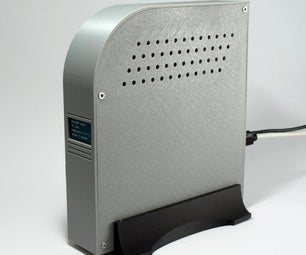
Introduction: Desktop Voltage Regulator/Power Supply
If you are an electronics student, hobbiest or pro you surely have the usual problem of supplying the right voltage to your devices and circuits.
This instructable will take you through the process of making a variable power supply (voltage regulator really) that is able to output 1volts to 17volts from 12volts 1000mA input (standard dc adapter).
The main schematic isnt mine but other than that its all my work, i also replaced the 1N5402 with 1N4007 since i didnt have the first available, the 4007 is much power full than the 5402 and it can handle up to 1000mA (which is our current rating), other than this diode every thing else is easy to find and available in most electronics shops.
Step 1: Materials
The following materials are needed for this project:
1x LM317 regulator
2x 1N4001 diode
1x 1N4007 diode
1x 1k resistor (for the led)
1x 220R resistor (R stands for 0 right hand zeros i.e. ohms)
1x 18k resistor
1x 470uF 40+ v electrolytic capacitor (minimum rating is 40v any thing higher is ok)
1x 470nF ceramic capacitor
1x 4.7uF 40+ v electrolytic capacitor
1x 10uF 40+ v electrolytic capacitor
1x 100n ceramic capacitor
1x LED (i used 5v blue LED so any thing between 1.5 and 5 will work and any color of course)
1x ON-ON switch (3 legs)
1x DC adapter jack
1x 10k potentiometer !!!LINEAR!!!
1x 4x7 cm blank PCB
Others:
Ferric Chloride etchant
Acetone
Glossy paper
I used some old computer screws to make stands for the board, so u r free to either use the idea or just get creative :)
Tools:
Water resistant marker (for fixing broken traces)
Laser Printer
PCB Drill
Solder iron
Solder
Cloth Iron
Step 2: The Schematics
As i mentioned before this is not my work, i just stumbled upon this schematic while browsing the web.
Attachments
Step 3: The PCB Design
This is the PCB design, i had to make this one on eagle since it wasn't supplied.
the powerPCB.pdf is a blank (no components visible), powerSchematic.pdf is for placement and powerSchematic2.pdf is a reference for placement (use it with the schematic to find out the components' values)
Step 4: Print the Board
Open up powerPCB.pdf and print the schematics on the glossy paper, remember to make it best quality and black cartridge for best results.
After you have printed the design, take your pcb and get a piece of steel wool and clean it under water until the copper shines, dry the pcb using a towel and then tape the cut design facing the copper on your board, this will ensure that the design stays consistent and dont move while we are transferring it over the board.
Now get your iron, set it up to the maximum temperature (for me it was linen mode) and start ironing over the paper until it stick to the board (the longer the better), dont try to remove the paper or you will damage the transferred design and you will have to acetone remove the transferred bits and start over again.
Soak the board with the paper taped (remove the tape first carefully) in hot water and start pealing off the paper until you are left with the copper board and the design transferred on top.
compare the board with the pcb design and using the marker fix any broken traces by covering the copper area with the marker.
Step 5: Etch the Board
Fill a plastic (!!!! not metal !!!!) container with just the amount of ferric chloride that covers your board, be careful to handle ferric chloride with extreme caution and wearing rubber gloves (this is an acid).
Now soak your board in the solution and start rocking the container side to side slowly until all the exposed copper is removed and you are left with a brown plastic a little bit lighter in color than the back of the board (if your board isnt brown just make sure the copper is totally removed by exposing the board to air for about 5 secs, if it turns pinkish its not yet removed).
Once done rinse your board with water and clean off any traces of FeCl.
Step 6: Clean the Design Off the Board
Now take the board and start cleaning off the design using a piece of cotton soaked in acetone, you will find it easily removed.
clean the board and then start comparing the result with the pcb design and identify any broken traces.
using your soldering iron solder the traces and test the connectivity (this is extremely important) then off you go to your drilling station.
Step 7: Drill and Place
Now take your pcb drill and start drilling your board in the correct places, be careful using the right drill bits for each hole, not that u can widen the holes as long as you make sure that the connection is still valid.
after drilling your board, turn it upside down and start placing the components as shown in powerSchematic.pdf, to identify the components use powerSchematic2.pdf and compare with the original schematic (sorry abt that i was just lazy to put the values after 5 times eagle screwing up my schematics and corrupting the save file).
Step 8: Solder
Now with all components placed, take your solder iron and start soldering the components, to make clean solders, take your soldering iron and heat the component leg then apply the solder wire to the leg (this will cause the solder to flow over the leg and copper pad giving a good solder and clean one too).
After soldering your components you r done :)
Step 9: Some Info
This regulator has the following features:
1 input port
2 output ports (1 for a digital voltmeter and the other for your devices)
regulation from 1.2 volts to 17.7 volts on 12 volt input (maximum output will vary according to the input)


