Introduction: Digitally Controlled 18W Guitar Amplifier


A couple of years ago, I built a 5W guitar amplifier, that was kind of solution to my audio system at the time, and recently I decided to build a new one much more powerful and without use of an analog components for the user interface, like rotary potentiometers and toggle switches.
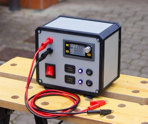
Digitally Controlled 18W Guitar Amplifier is a stand-alone, digitally controlled 18W mono guitar amplifier with delay effect system attachment and an elegant liquid-crystal display, providing exact information what is going on in the circuit.
The features of the project:
- Fully digital control: User interface input is a rotary encoder with a built in switch.
- ATMEGA328P:Is a micro-controller (used as Arduino-like system): All the adjustable parameters are controlled programatically by the user.
- LCD:acts as a user interface output, so the device parameters such as gain/volume/delay depth/delay time can be observed in great approximation.
- Digital Potentiometers: Are used in the sub-circuits thus making device control fully digital.
- Cascaded system: Each circuit in the pre-defined system is a separate system that shares only power supply lines, capable of relatively easy troubleshooting in the case of failures.
- Pre-amplifier: Based on LM386 integrated circuit, with very simple schematic design and minimum parts requirement.
- Delay effect circuit: Is based on PT2399 integrated circuit, can be purchased from the eBay as a separate IC (I designed the whole delay circuit myself) or can be used as a complete module with ability to substitute rotary potentiometers with digipots.
- Power amplifier: Is based on TDA2030 module, that is already contains all the peripheral circuits for its operation.
- Power supply: Device is powered by old external laptop 19V DC power supply, thus device contains a step-down DC-DC module as a pre-regulator for the LM7805 making it dissipate much less heat during device power usage.
After we've covered all the brief information, let's build it!
Step 1: The Idea


As you can see in the block diagram, device operates as classical approach to the guitar amplifier design with slight variations on the control circuit and user interface. There is total of three groups of circuits that we will expand about: Analog, digital and power supply, where each group consists of separate sub-circuits (the topic will be well explained in the further steps). To make it much easier to get into understanding the project structure, let's explain those groups:
1. Analog Part: Analog circuits are located in the upper half of the block diagram as it can be seen above. This part is in charge for all the signals that pass through the device.
1/4" jack is a device' guitar mono input and is located at the boundary between box and soldered electronic circuit.
The next stage is a pre-amplifier, based on LM386 integrated circuit, which is extremely easy to use in such audio applications. LM386 is supplied 5V DC from the main power supply, where its parameters, gain and volume, are controlled via digital potentiometers.
The third stage is power amplifier, based on TDA2030 integrated circuit, powered by external 18~20V DC power supply. At this project, gain that is selected on the power amplifier remains constant for all the operation time. Since device is not a single wrapped up PCB, it is recommended to use TDA2030A assembled module, and attach it to the prototype bard with connecting only I/O & power supply pins.
2. Digital Part: Digital circuits are located in the lower half of the block diagram. They are in charge for user interface and analog parameters control such as delay time/depth, volume and gain..
Encoder with built-in SPST switch is defined as a user control input. Since it is assembled as a single part, the only need for proper operation is attaching pull-up resistors programatically or physically (We'll see it in the schematics step).
Microprocessor as the "main brain" in the circuit is ATMEGA328P, that is used in Arduino-like style in this device. It is the device that has all the digital power over the circuitry, and commands everything what to do. Programming is done via SPI interface, so we can use any appropriate USB ISP programmer or purchased AVR debugger. In the case you want to use Arduino as the microcontroller in the circuit, this is possible through compiling attached C code that is present in the programming step.
Digital potentiometers are a couple of double integrated circuits controlled via SPI interace by microcontroller, with total number of 4 potentiometers for full control over all the parameters:
LCD is a user interface output, that lets us know what is happening inside the box. In this project I used probably most popular 16x2 LCD among Arduino users.
3. Power Supply: Power supply is in charge to give energy (Voltage and current) to the whole system. Since power amplifier circuit is powered straight from external laptop adapter and all the remaining circuits are powered from 5V DC, there is need for a DC-DC step-down or linear regulator. In the case of putting 5V linear regulator connecting it to the external 20V, when current passes through linear regulator to the load, a huge amount of heat dissipated on the 5V regulator, we don't want that. So, between 20V line and 5V linear regulator (LM7805), there is 8V DC-DC step-down converter, that acts as a pre-regulator. Such attachment prevents huge dissipation on linear regulator, when load current achieves high values.
Step 2: Parts and Instruments


Electronic Parts:
1. Modules:
- PT2399 - Echo\delay IC module.
- LM2596 - Step-down DC-DC module
- TDA2030A - 18W Power mmplifier module
- 1602A - Common LCD 16x2 characters.
- Rotary encoder with embedded SPST switch.
2. Integrated Circuits:
- LM386 - Mono audio amplifier.
- LM7805 - 5V Linear regulator.
- MCP4261/MCP42100 - 100KOhm dual digital potentiometers
- ATMEGA328P - Microcontroller
3. Passive Components:
A. Capacitors:
- 5 x 10uF
- 2 x 470uF
- 1 x 100uF
- 3 x 0.1uF
B. Resistors:
- 1 x 10R
- 4 x 10K
C. Potentiometer:
- 1 x 10K
(Optional) If you are not using PT2399 module, and interested in building the circuit yourself, these parts are required:
- PT2399
- 1 x 100K Resistor
- 2 x 4.7uF Capacitor
- 2 x 3.9nF Capacitor
- 2 x 15K Resistor
- 5 x 10K Resistor
- 1 x 3.7K Resistor
- 1 x 10uF Capacitor
- 1 x 10nF Capacitor
- 1 x 5.6K Resistor
- 2 x 560pF Capacitor
- 2 x 82nF Capacitor
- 2 x 100nF Capacitor
- 1 x 47uF Capacitor
4. Connectors:
- 1 x 1/4" Mono jack connector
- 7 x Double terminal blocks
- 1 x Female 6-pin row connector
- 3 x 4-pin JST connectors
- 1 x Male power connector jack
Mechanical Parts:
- Speaker with power acceptance equal or greater than 18W
- Wooden enclosure
- Wooden frame for user interface cut-away (For LCD and rotary encoder).
- Foam rubber for speaker and UI areas
- 12 drill screws for the parts
- 4 x fastening bolts and nuts for LCD frame
- 4 x rubber leg for steady device oscillations (Resonance mechanical noise is a common thing in the amplifier design).
- Knob for rotary encoder
Instruments:
- Electric screwdriver
- Hot-glue gun (If necessary)
- (Optional) Lab power supply
- (Optional) Oscilloscope
- (Optional) Function generator
- Soldering iron\station
- Small cutter
- Small Plier
- Soldering tin
- Tweezers
- Wrapping wire
- Drilling bits
- Small-sized saw for wood cutting
- Knife
- Grinding file
Step 3: Schematics Explanation


Since we are familiar with the block diagram of the project, we can proceed to the schematics, taking in account all the things we need to know about circuit operation:
Pre-Amplifier Circuit: LM386 is connected with minimum parts consideration, with no need to use external passive components. In the case you want to change frequency response to the audio signal input, like bass boost or tone control, you can refer to the LM386 datasheet, speaking of which, will not affect this device schematic diagram except for pre-amplifier slight changes in connections. Since we are using a single 5V DC supply for the IC, decoupling capacitor(C5) has to be added to the output of the IC for the DC removal of the signal. As it can be seen, 1/4" connector(J1) signal pin is connected to the digipot 'A' pin, and LM386 non-inverting input is connected to the digitpot 'B' pin, so as a result, we have simple voltage divider, controlled by microcontroller via SPI interface.
Delay\Echo Effect Circuit: This circuit is based on PT2399 delay effect IC. This circuit seems complicated according to its datasheet, and it is very easy to get confused with soldering it altogether. It is recommended to purchase complete PT2399 module that is already assembled, and the only thing to do is to desolder rotary potentiometers from the module and attach digipot lines (Wiper, 'A' and 'B'). I've used a datasheet reference to the echo effect design, with digipots attached to the oscillations time period selection and volume of the feedback signal (What we should call - "depth"). Delay circuit input, referred as DELAY_IN line is connected to the output of the pre-amplifier circuit. It is not mentioned in the schematics because I wanted to make all the circuits to share only power lines, and signal lines are connected with external cables. "How not convenient!", you may think, but the thing is, when building an analog processing circuit, it is much easier to troubleshoot part by part each circuit in the project. It is recommended to add bypass capacitors to the 5V DC power supply pin, because of its noisy area.
Power Supply: Device is powered via external power jack by 20V 2A AC/DC adapter. I found that best solution to reduce large amount of power dissipation on a linear regulator in the form of heat, is to add 8V DC-DC step-down converter(U10). LM2596 is a buck converter used in many applications and popular among Arduino users, that costs less than a 1$ on the eBay. We know, that linear regulator has a voltage drop on its throughput (in the case of 7805 theoretical approximation is around 2.5V), so there is a secure gap of 3V between input and output of the LM7805. It is not recommended to neglect linear regulator and connect lm2596 straight to the 5V line, because of the switching noise, which voltage ripple can affect circuits power stability.
Power Amplifier: It is simple as it seems. Since I've used a TDA2030A module in this project, the only requirement is to connect power pins and I/O lines of the power amplifier. As it was mentioned before, power amp's input is connected to the delay circuit output via external cable using connectors. Speaker that is used in the device is connected to the output of the power amplifier via dedicated terminal block.
Digital Potentiometers: Probably most important components in the whole device, making it capable being controlled digitally. As you can see there are two types of digipots: MCP42100 and MCP4261. They share the same pinout but differ in communication. I've got only two last digipot in my stock when I've built this project, so I just used what I had, but I recommend to use two digipots of the same type either MCP42100 or MCP4261. Each digipot is controlled by an SPI interface, sharing clock(SCK), and data input(SDI) pins. SPI controller of the ATMEGA328P is capable handling multiple devices by driving separate chip select (CS or CE) pins. It is designed that way in this project, where SPI chip enable pins are connected to separate microcontroller pins. PT2399 and LM386 are connected to 5V supply, so we don't need to worry about voltage swing on digipot resistor network inside the ICs (It is covered largely in the datasheet, in the section of voltage level range on inner switching resistors).
Microcontroller: As it was mentioned, based in an Arduino-style ATMEGA328P, with the need of single passive component - pull-up resistor (R17) on the reset pin. 6-pin connector (J2) is used for device programming via USB ISP programmer through SPI interface (Yes, the same interface that digipots are connected to). All the pins are connected to the appropriate components, which are presented in the schematic diagram. It is strongly recommended to add bypass capacitors near the 5V power supply pins. The capacitors you see near the encoder pins (C27, C28) are used to prevent encoder state bouncing on these pins.
LCD: Liquid crystal display is connected in a classic way with 4-bit data transmission and additional two pins of latching the data - Register select (RS) and Enable (E). LCD has a constant brightness and variable contrast, that can be adjusted with a single trimmer (R18).
User Interface: Device' rotary encoder has a built-in SPST push button, where all its connections are tied to the described microcontroller pins. It is recommended to attach pull-up resistor to each encoder's pin: A, B and SW, instead of using internal pull-up. Make sure that encoder A and B pins are connected to the microcontroller external interrupt pins: INT0 and INT1 to conform device' code and reliability when using the encoder component.
JST Connectors and Terminal Blocks: Each analog circuit: pre-amplifier, delay and power amplifier are isolated on the soldered board and are connected with cables between the Terminal Blocks. Encoder and LCD are attached to the JST cables and connected to the soldered board via JST Connectors as described above. External power supply jack input and 1/4" mono jack guitar input are connected via terminal blocks.
Step 4: Soldering


After a brief preparation, there is need to imagine precise placement of all the components on the board. It is preferred to begin the soldering process from the pre-amplifier, and finish with all the digital circuitry.
Here's step-by-step description:
1. Solder pre-amplifier circuit. Check its connections. Make sure that ground lines are shared on all the appropriate lines.
2. Solder PT2399 module/IC with all the peripheral circuitry, according to the schematic diagram. Since I've soldered the whole delay circuit, you can see that there are a lot of shared lines that capable of being soldered easily according to each PT2399 pin function. If you have a PT2399 module, then just desolder the rotary potentiometers and solder digital potentiometer net lines to these freed pins.
3. Solder TDA2030A module, make sure that speaker output connector is face centered outside the board.
4. Solder power supply circuit. Place bypass capacitors according to the schematics diagram.
5. Solder Microcontroller circuit with its programming connector. Try to program it, make sure it doesn't fail in the process.
6. Solder digital potentiometers
7. Solder all the JST connectors in the areas according to each line connection.
8. Power up the board, if you have a function generator and oscilloscope, check each analog circuit response to the input signal step-by-step(recommended: 200mVpp, 1KHz).
9. Check circuit's response on power-amplifier and delay circuit/module separately.
10. Connect speaker to the output of power amplifier and signal generator to the input, make sure you hear the tone.
11. If all the tests we've conducted are successful, we can proceed to the assembly step.
Step 5: Assembly


Probably this is the hardest part of the project from the point of view of technical approach, unless there are some useful tools for the cutting wood in your stock. I had a very limited set of instruments, so I was forced to go the tough way - cutting box manually with a grinding file. Let's cover the essential steps:
1. Preparing the box:
1.1 Make sure you have wooden enclosure with appropriate dimensions to the speaker and electronic board allocation.
1.2 Cut the region for the speaker, it is strongly recommended to attach foam rubber frame to the speaker cut-out area to prevent resonance vibrations.
1.3 Cut separate wooden frame for the user interface (LCD and encoder). Cut off appropriate area for the LCD, make sure that LCD direction is not inverted to the front enclosure view. After this is completed, drill a hole for rotary encoder. Fasten LCD witch 4 drilling screws and rotary encoder with a appropriate metallic nut.
1.4 Place foam rubber on the user interface wooden frame on its whole perimeter. This will help preventing resonating notes as well.
1.5 Locate where electronic board will be located, then drill 4 holes on the wooden enclosure
1.6 Prepare a side, where DC external power supply input jack and 1/4" guitar input will be located, drill two holes with appropriate diameters. Make sure these connectors share the same pinout as the electronic board (i.e polarity). After that, solder two pairs of wires for each input.
2. Connecting the parts:
2.1 Attach speaker to the selected area, make sure two wires are connected to the speaker pins with 4 drilling screws.
2.2 Attach user interface panel on the selected side of the enclosure. Don't forget the foam rubber.
2.3 Connect all the circuits together via terminal blocks
2.4 Connect LCD and encoder to the board via JST connectors.
2.5 Connect speaker to the TDA2030A module output.
2.6 Connect power and guitar inputs to the terminal blocks of the board.
2.7 Locate the board at the drilled holes' position, fasten board with 4 drilling screws from outside the wooden enclosure.
2.8 Attach all the wooden enclosure parts all together so it will look like a solid box.
Step 6: Programming and Code
Device code obeys the rules of AVR microcontrollers family and conforms ATMEGA328P MCU. The code is written in Atmel Studio but there is an opportunity to program Arduino board with Arduino IDE that has the same ATMEGA328P MCU. Stand-alone microcontroller can be programmed via USB debug adapter with accordance with Atmel Studio or via USP ISP programmer, that can be bought from eBay. Programming software that is commonly used is AVRdude, but I prefer a ProgISP - simple USB ISP Programming software with a very friendly user interface.
All the needed explanation about the code, can be found in the attached Amplifice.c file.
Attached Amplifice.hex file can be uploaded straight to the device if it fully conforms the schematic diagram that we've been observing previiously.
Attachments

Step 7: Testing


Well, after everything that we wanted is done, it's time for testing. I preferred to test device with my ancient cheap guitar and simple passive tone control circuit that I've built years ago for no reason. Device is tested also with both digital and analog effects processor. It's not too great that PT2399 has such a small RAM for storing audio samples used in delay sequences, when time between echo samples is too large, echo becomes digitized with a great loss of transition bits, what is considered as distortion of signal. But that "digital" distortion that we hear, may be useful as a positive side effect of the device operation. It all depends on the application you want to make with this device (which somehow I called "Amplifice V1.0" by the way).
Hope you'll find this instructable useful.
Thanks for reading!