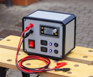
Introduction: Function Generator


This instructable describes the design of function generator based on the Maxims's Analog integrated circuit MAX038.
The function generator is very useful tool for the electronics freaks. It is needed for tuning resonance circuits, testing audio and video equipment, designing of analog filters and for many other different purposes.
Today there are two main types of function generators ; digital, (DSP based, DDS...) which are more and more often used and analog, which were the origins.
Both types have their advantages and disadvantages. The digital generators can generate signals with very stable frequency, but they have problems with generating very pure sine signals (what is not problem for analog one). Also the mainly spread function generators based on DDS approach have not so big frequency generation range.
Since long time I wanted to design a useful function generator, which could somehow combine some of the advantages of both types (analog and digital) generators. I decided to base the design on the Maxim chip MAX038*
* Remark - this chip is no more produced and sold by Maxim. It is obsolete. It is still possible to find it in eBay, Aliexpress and other sites for electronic components.
There are existing also other analog function generator chips (XR2206 from Exar, icl8038 from Intersil), but I had
one MAX038 available, and I used it. The digital features of the function generator were performed by one Atmega328 chip. Its functions are the following:
- controls the frequency range selection
- controls the signal type (sine, rectangular, triangular, sawtooth)
- measures the amplitude of the signal
- measures the DC offset
- measures the frequency of the signal
- measures the THD of the sine signal in the audio range (this still have to be implemented)
- displays all this information on a character 16x2 LCD display.
Step 1: MAX038 Description

I have attached the MAX038 datasheet.There can be seen the most important chip parameters:
♦ 0.1Hz to 20MHz Operating Frequency Range
♦ Triangle, Sawtooth, Sine, Square, and Pulse Waveforms
♦ Independent Frequency and Duty-Cycle Adjustments
♦ 350 to 1 Frequency Sweep Range
♦ 15% to 85% Variable Duty Cycle
♦ Low-Impedance Output Buffer: 0.1Ω
♦ Low 200ppm/°C Temperature Drift
Another important requirement is the need of dual supply (±5V). The output amplitude is fixed (~ 2 VP-P with 0 V DC offset).
On the page 8 of the datasheet can be seen the block-diagram of the chip. On page 11 can be seen the simplest circuit, which can be used for generating of sine wave signal. This circuit was taken as basis for the design of the function generator.
Attachments

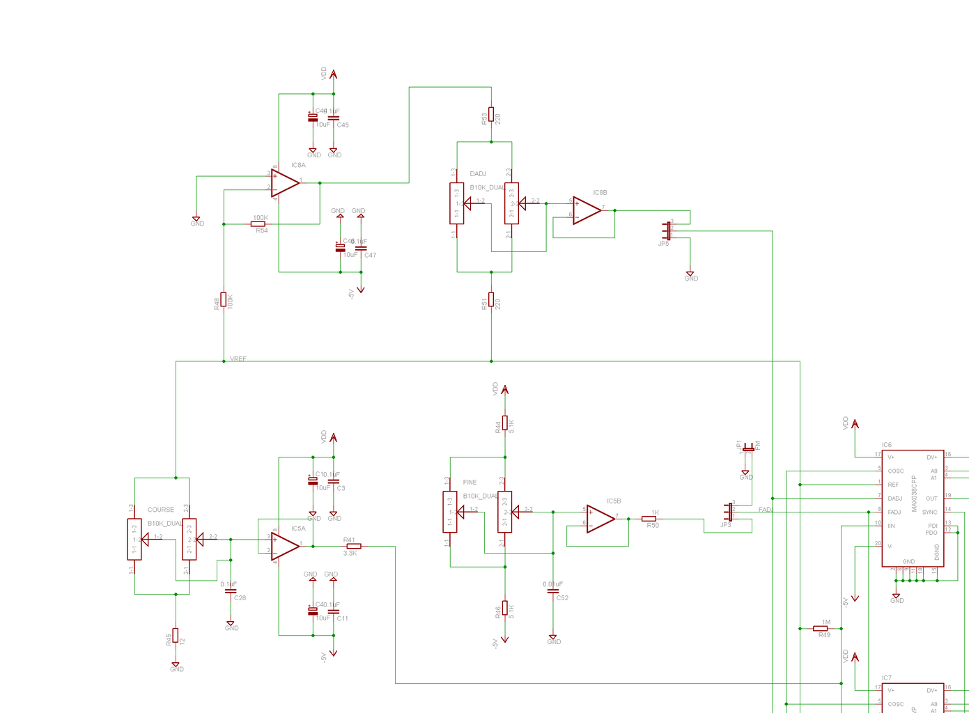
Step 2: The Circuit ....
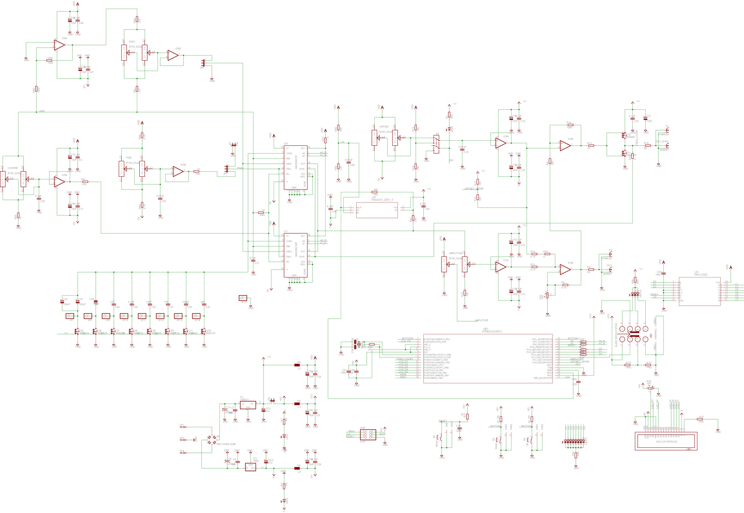
On the picture is presented the circuit of the function generator I did this image with highest possible resolution to guarantee that each .device value can be read properly. The schematics looks quite complex and to be understood better I will explain its main parts separately. Many readers could blame me that the circuit is too redundant. That is true. At first you can see that it contains two MAX038 chips. The reason is that the PCB supports both type of packages SO and DIP. The redundancy can be seen also in some functions -
1)LED's show the current active frequency range, but it also is displayed on the LCD;
2)LED's are used also to indicate the signal type, but also the LCD shows this information
The design is done in this way to allow more flexibility to the user - under desire he could not use the LCD, or simply can omit the soldering of LED's. I have soldered them to be able to debug the functionality during the design phases.
It can be noticed also that I use a lot of opamps. Some of them can be omitted without problems - especially the buffers. In the present time the opamps by their self offer big redundancy - in one package you can find 2, 4 even 8 separate amplifiers, and this at relatively low price. Why not to use them?
Redundant are also the filtering capacitors - each analog chip used has its own capacitor bank ( tantalum + ceramic capacitors for both supplies). Some of them can be also omitted.
Attachments

Step 3: Circuit Explanation - Power Supply (1)

As I said this generator requires dual supply. The positive voltage is created by the use of 7805 linear voltage regulator. The negative supply is generated by 7905 chip. The middle tap point of the 2x6V transformer is connected to the common ground of the board. The generated power supplies - both the positive and the negative are separated to analog and digital by chocks. Two LEDs indicate the presence of each supply.
Step 4: Circuit Explanation - Frequency Range Control (2)
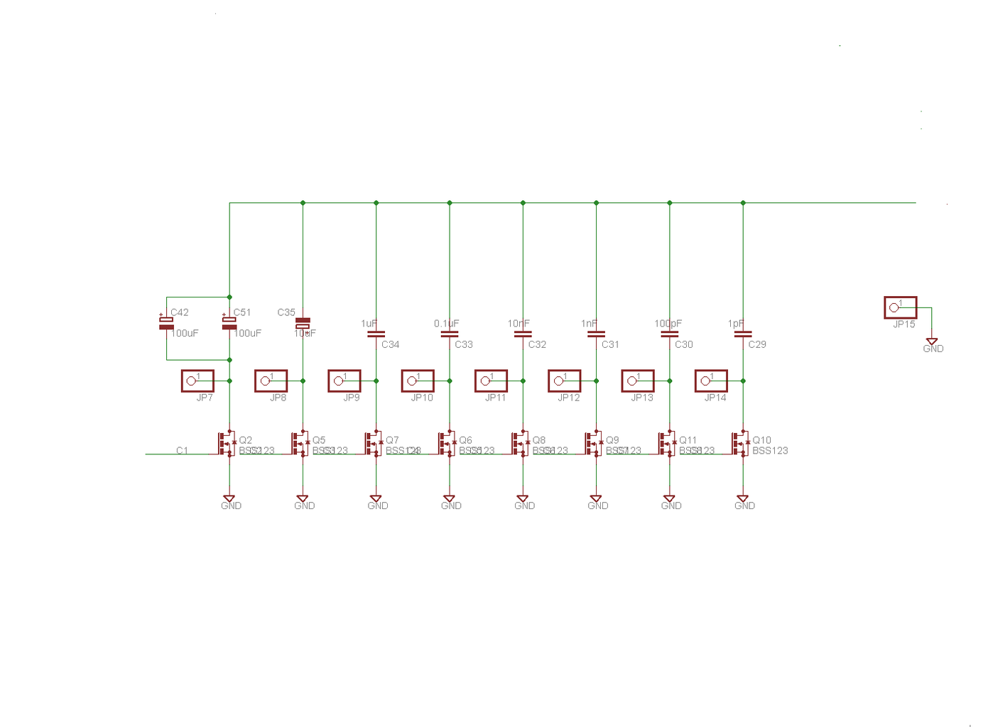
To cover big frequency range a multiple capacitor bank is used. The capacitors have different values and they define different frequency sub-ranges.Only one of these capacitors is used during the work - its bottom plate is grounded by MOS transistor switch. Which capacitors bottom plate to be grounded is controlled by the Atmega328 by the use of demultiplexer chip 74HC238. As MOS switches I used BSS123 transistors. The main requirement for this switch is to have low Ron and the lowest possible drain capacitance. The digital control of the capacitor bank can be omitted - the PCB contains holes for soldering the wires for mechanical rotary switch.
Step 5: Circuit Explanation - the Frequency Adjustment (3)
On the picture are shown the frequency and duty cycle control circuity. There I used the standard LM358 opamp (dual amplifier in one package). I used also dual 10K potentiometers.
The MAX038 chip generates internal voltage reference 2.5V, which is used normally as reference for all adjustments.
This voltage is applied at the inverting input of IC8a and it generates negative voltage reference used for the DADJ (duty cycle adjustment). Both voltages are applied at the potentiometer for the DADJ, which middle tap is buffered and applied to the DADJ pin of the MAX038 chip. The jumper JP5 can be used to disable the DADJ function, when connected to ground. The "Course" frequency control is preformed by changing the current sunk / sourced in MAX038 "IIN" pin. This current is defined by the resistor R41 and the output voltage of the opamp buffering the middle tap of the course frequency control potentiometer. All these can be replaced by single potentiometer (in reostat connection) between the REF and IIN MAX038 pins.
Step 6: Circuit Explanation - Amplitude Control, SYNC Signal Generation... (4)


As written in the datasheet the output signal pf the MAX038 has amplitude ~1 V with DC voltage equal to the ground potential.
I wanted to have the possibility to control the signal amplitude and to be able to define the DC offset by myself. As additional feature I wanted to have SYNC signal with CMOS levels in parallel with the output signal. By default the MAX038 chip generates such signal, but in the datasheet I read that if this feature is enabled (what means - DV+ pin connected to 5V), some peaks (noise) can be observed in the output analog signal.I wanted to keep it as clean as possible and for that reason I generated the SYNC signal externally. The PCB is done in the way that the DV+ pin can be bridged easily to the main supply. The SYNC pin is routed to the BNC connector - only 50 Ohm resistor must be soldered. In this case, the SYNC signal generation circuitry can be omitted. Here as you see I use also dual potentiometers, but they are not connected in parallel. The reason for that is - I measure the amplitude relatively. The voltage at the middle point of one potentiometer is sensed by the Atmega328 ADC and the signal amplitude is calculated based on this value. Of course this method is not very precise (it relies on the matching of both potentiometer sections, which not always occurs), but it is enough precise for my applications. In this circuit IC2A is working as voltage buffer. IC4A also. The IC2B opamp works as summing amplifier - it creates the output signal of the functional generator as sum of the offset voltage and the main signal with adjusted amplitude.The voltage divider R15.R17 generates suitable voltage signal for measuring the DC main signal offset. It is sensed by the Atmega328 ADC. The IC4B opamp works as comparator - it controls the SYNC generation inverter realized by the two MOS transistors (BSS123 and BSS84). The U6 (THS4281 - Texas Instruments) shifts the output signal generated by the MAX038 DC with 2.5 V and amplifies it 1.5 times. So generated signal is sensed by the AVR ADC and processed further with FFT algorithm. In this part I used high quality rail to rail opamps with 130 MHz bandwidth (TI - LMH6619).
To be easy to understand how exactly the SYNC signal generation, works I am including some pictures of LTSpice simulations of the circuit. On the third picture: the blue signal is the offset voltage (input of the IC2B). The green one is the output signal with adjusted amplitude. The red one is the output signal of the functional generator, The cyan curve is the SYNC signal.
Step 7: PCB Design

I used "Eagle" for the designing of the PCB. I ordered the PCB's at "PCBway". Them took only four days to produce the boards and a week to deliver them. Their quality is high, and the price is extremely low. I paid only 13 USD for 10 PCBs!
In addition to that I could order a different colour PCBs without price increase. I have chosen yellow ones :-).
I am attaching the gerber files according to the "PCBway" design rules.
Attachments
Step 8: Soldering

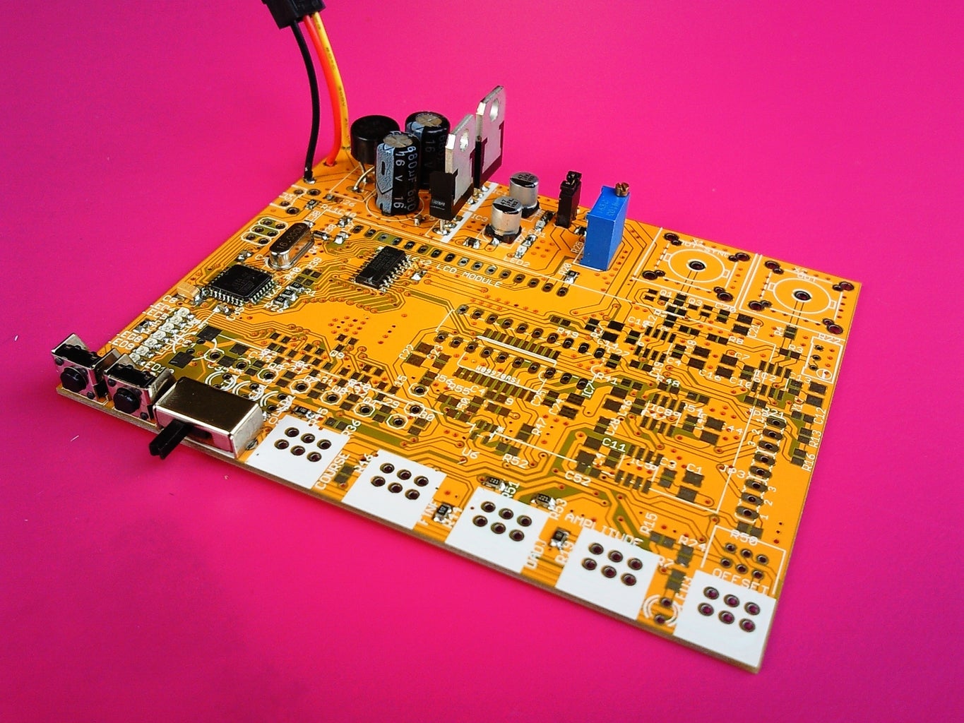


First I soldered the power supply circuitry devices..
After testing the supply block, I have soldered the Atmega328 chip with its supporting devices : quartz crystal, capacitors, filtering caps and the ISP connector. As you see I have a jumper in the supply line of the AVR chip. I disconnect it when I program the chip through the ISP. I use USBtiny programmer for that purpose.
As next step I soldered the de-mux chip 74HC238, the LED's indicating the frequency range. I loaded a small Arduino program in the Atmega chip, which was testing the multiplexing. (see the video under the link above)
Step 9: Soldering...


As next step I soldered the opamps working in the DC mode (LM358) and the frequency and DADJ adjustment potentiometers and checked all their functions.
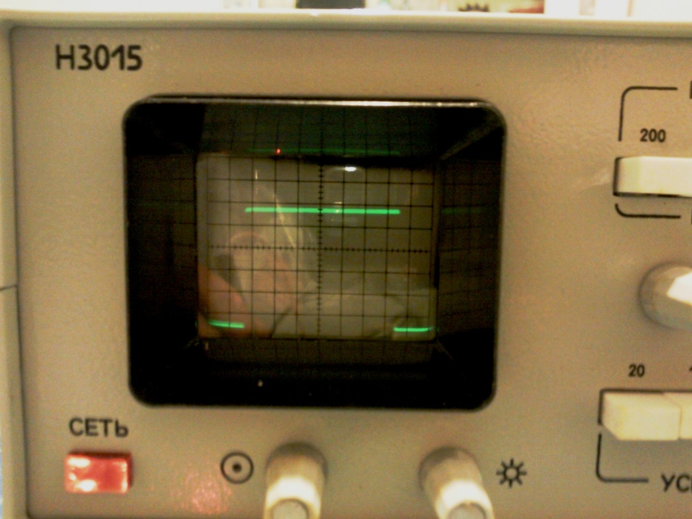
Further I soldered the BSS123 switches, the frequency determining capacitors and the MAX039 chip. I tested the functional generator probing the signal at the native chip signal output. (You can see my old Soviet, produced 1986, still working oscilloscope in action :-) )
Step 10: More Soldering...


After that I soldered the socket for the LCD display and tested it with the "Hello world" sketch.
I soldered the other remaining opamps, capacitors, potentiometers and the BNC connectors.
Step 11: Software

For creating of the Atmega328 firmware I used the Arduino IDE.
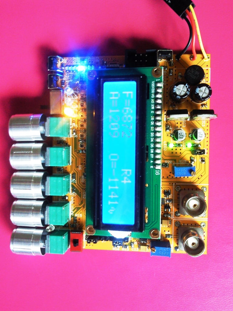
For the frequency measurement I used the "FreqCounter" library. The sketch file and the used library are available for download. I have created special symbols to represent the currently used mode (sine, rectangular, triangle).
On the picture above can be seen the information shown on the LCD:
- Frequency F=xxxxxxxx in Hz
- Frequency range Rx
- Amplitude in mV A=xxxx
- Offset in mV 0=xxxx
- type of the signal x
The function generator has two push buttons on the front in the left side - they are used the change the frequency range (step up -step down). In the right of them is the slide switch for the controlling of the mode, after it from left to right follow the potentiometer for the controlling of the frequency ( course, fine, DADJ) , amplitude and the offset. Close to the offset adjustment potentiometer is placed the switch used to commutate between the fixed at 2.5V DC offset and the tuned one.
I have found a small error in the "Generator.ino" code in the ZIP file - the symbols for sine and triangle wave forms were swapped. In the single "Generator.ino" file attached here, the error is corrected.
Attachments
Step 12: To Be Done ...
As last step I intend to implement additional feature - measurement of the THD of the audio frequency sine signal in real time using FFT. This is needed, because the duty cycle of the sine signal could differ from 50%, what can be caused by internal chip mismatches and other reasons and could create harmonic distortions. The duty cycle can be adjusted by the potentiometer, but without observing the signal on the oscilloscope or spectrum analyser it is impossible to trim fine its shape. Calculating the THD based on the FFT algorithm could solve the problem. The result of the THD calculations will be displayed on the LCD in the top right empty space.
On the video can be seen the spectrum of the generated by the MAX038 sine signal. The spectrum analyser is based on Arduino UNO board + 2.4" TFT shield. The spectrum analyser uses the SpltRadex Arduino library developed by Anatoly Kuzmenko to perform FFT in real time.
I still did not decide - to use this library or to use the FHT library created by the Musiclabs.
I intend to use the information taken from the frequency meter measurements to calculate the proper sampling window and to suspend the use of additional windowing during the FFT calculations. I need only to find some free time to make this happen. I hope to have some results soon....