Introduction: Hand Controlled System


Main idea
In this project, we would like to develop a wearable system which will be able to control some different device, such as a robot, or a computer without using any ordinary PC peripherals. We embedded one gyroscope into a ring and one into a wrist strap.
The base of the ring and wrist strap is an FPGA board, what will process the gestures. With a gesture of our fingers or our wrist, we will realize the control. The main idea of this project is to speed-up and to help the user’s activities. This will be a multifunctional hardware. It will be useful for learning, reading, gaming or for people with handicaps.
Motivation
This project is made for the Digilent Design Contest, and this is the beginning form of our final system.
Main devices what we used:
- CmodA7 FPGA board
- 2x Pmod NAV : 9-axis IMU
- 2x Pmod BT2: Bluetooth Interface
- Zybo Zynq-7000 ARM/FPGA SoC Trainer Board
- Vivado 16.4
Implementation
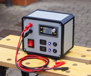
The main control unit of the project the Zybo board.We installed xillinux operating system for Zybo. On board, we design those input devices that are required for presentation devices, such as UART for Bluetooth or VGA for the monitor.
Another important unit of the project is the control unit which is on the user’s hand. We implemented a hand tracking and a motion detection with the accelerometer + gyroscope. The user who wear the devices on his wrist and his fingers, therefore, the devices will detect more complex motions. On the wrist, the user wears a Cmod A7 FPGA, an NAV-IMU. During the movement, the values of the sensor are transmitted to the Zybo via Bluetooth. The Zybo is able to handle and processes the incoming sensor data. The wrist-mounted command system converts the data using a specific protocol system. Those devices that we have to control need to have protocol processing routines. The protocol contains all information about the hand movement as its speed and directions. Therefore we need more measurements and analyses of data traffic.
Before you start to replicate this project please read carefully these tutorials and manuals
Step 1: Before You Start
Getting started with Vivado
First of all, start this project with installing Vivado 16.4 This software contains a Hardware Development Kit which helps you to build your own MicroBlaze processor into the CmodA7 FPGA, and also contains a Software Development Kit to program your built-in processor.
Setup your environment
The Vivado by defaults doesn't contain any CmodA7 board files, so add these files to the environment based on this tutorial. It's an easy copy + paste operation.
When you finished the tutorial, you can choose the CmodA7 board in the new project window. The Vivado doesn't contain IP's to CmodA7 by defaults, so you need to add it too. Download these IP's from here, we will use it later.
Step 2: Create MicroBlaze
Next step, you should create a MicroBlaze processor and embed it to the CmodA7. The Digilent has a complete and so detailed tutorial, how to do this. Follow it carefully, while you reach the 3.2 paragraph "Run Block Automation".
In this window, you can choose how many program memory and cache memory you want to use. Later, when you program your logic in C language, you need a pretty big memory capacity to allocate and store all drivers and operate with these. To avoid these mysterious memory errors later in SDK choose the following configurations
- Local Memory 128 kB
- Local Memory ECC: None
- Cache Configuration: 8 kB
- Debug Module: Debug only
- Peripheral AXI Port: Enabled
- Interrupt Controller: Enable
Follow the tutorial up to the 5. paragraph "Adding Peripheral Components", because after this step we want to build in some sweet thing into the block design.
Step 3: Create the Block Desing


CmodA7 IPs
Now your block design looks similar like on the first picture. In this step, you need to add the Pmod IPs which you downloaded in the first step. Follow this tutorial while you reach the 2.2 paragraph. After you added these components just right click somewhere on the block diagram, and start to type "Pmod". Add from the list 2 piece of PmodNav IP, a PmodBT2 IP and an axi_quad_spi IP. If you created an interrupt control in the second step, just click on "Run connection automation", if not, add a xlconcat IP and a axi_intc IP to the block desing, then click "Run connection automation"
Wire up these things
There is some wire what you need to connect by hand. First, these Pmod IP's has an Interrupt pin. Wire up these output pins with the Concat IP input pins. Wire up the xlconcat IP dout[2:0] output with the axi_intc s_axi input, then the axi_intc interrupt output with the Microblaze Interrupt. When you finished, your block design looks like similar then the second picture.
Add external port
By default, the Pmod IPs want to use the CmodA7 JA connector pins to operate through these. In this part you need to make these IPs output external. Right click on each Pmod IPs output and from the list choose "Make external" option. Vivado will create a Pmod_out connector for you. Because now nobody knows where do you want to put these pins physically, you need to create a constraint file. In this file bind all pins physically on the device, what you planning to use. To do this, create an XDC file in the source window, and copy-paste the CmodA7 master XDC from here
Edit the XDC
All IP on the block design has own XDC, which contains a default pin location and binding. Uncomment your XDC file just those lines, which you really want to modify. These lines are located in the GPIO section. My own looks like on the third picture. This is a user defined pinout so be careful when you edit the XDC. To help you, I added the fourth picture which describes the CmodA7 Package_Pin names and its physical location.
Step 4: Store Your Code in RAM
Congratulations! If you reached this step, you have a working processor on CmodA7 with the required peripherals. Now, when you create a program on the module, this will run until you unplug all power sources. Our objective is to create a memory which is able to store our program and after plugging in the power source, this program starts automatically.
Create a program memory
After you are done with the "Generate Bitstream" or the "Run implementation" a popup window appears. Click on the "Open implemented design". Follow this tutorial 0-th step to do some changes on the bitstream settings. After then click on "Generate Bitstream" again. This will create you a compressed bitstream. This step is really important because of the limited memory capacity of the Cmod made for.
Launch SDK
Follow this tutorial to launch SDK. 7-10 paragraph. Create the sample "Hello Word"
Step 5: Inside the SDK
Use the Pmod drivers
In this step, your SDK project contains the PmodNAV and the PmodBT2 drivers. The SDK imported these for you. Because the PmoNAV is the newest product of Digilent, it doesn't have full support yet, and the driver library which was made for it is a bit weird and corrupted. You can't build this project, so let's change these libraries.
Read carefully this forum post, and replace your corrupted PmodNAV files with those, what jpeyron published in his last comment. Copy and replace these files content with yours. Because of this device drivers and libraries are under development, maybe you don't get the corrupted drivers, and the Digilent guys solved the problem.
You can see some really useful examples near these files, deep dive a bit into the project hierarchy.
Upload the project permanently
To upload permanently your project need to do some project setting. Follow this tutorial 1.4 to 1.6 paragraphs. Don't create SREC Bootloader API project, just do these steps on your own project. Click on "Program FPGA" and instead of "bootloop" choose the "microblaze_0" software configuration which is your project's elf. This will create for you a "download.bit" file. This is why we worked for. My project name is "all_in_one" so in the directory structure there is an "all_in_one.elf" file.
After this step:
- click on "Program Flash" and browse the "download.bit" file which located in "system_wrapper_hw_platform_0" folder.
- The offset is 0x0 since the program start to running from the 0 Th memory address.
- Choose your flash type (n25q32-3.3V)
- Check in all checkbox and program
Upload the project temporarily
If you want just test your project on the FPGA, simple click on the green "Play" button ad enjoy!
Step 6: Set Up Linux on Zybo
To help for those, who want to use Linux on Zybo, we created several pre-built ISO images. In this part, I show you, how to use these on a concrete example. In this project, we used "xillinux_zybo.img" from here.
SD cards
This image size is 7,4 GB, so you need a 8 GB SD card or bigger to use this system. First, format the SD card
- Use GParted if you use Linux operating system
- Use EaseUS partition tool if you use Windows
Format the SD card to FAT32. Download the Win32 Disk imager from here and write the ISO image to the card with it. That's all, the Zybo Linux is works.
We pre-built some other Linux image with different input and output pins and logic. If you just starting to learn Zybo, this is a powerful choice for you. This is the simplest way if you want to replicate our project.
Step 7: Additional Configurations and Resources
Set up the Bluetooth
The Pmod BT2 interface is a powerful tool if you want to transfer short data from one device to another in a simple way. These modules use UART communication, and they can auto connect to each other. This tutorial shows you, how.
Resources
Finally, here is a link to our project. The full documentation is not ready yet, as I told this is the beginning form of our project. If you have any question, leave a comment and we reply as soon as possible.