

Introduction: My PCB Making


So this Lazy Old Geek (LOG) decided to start making my own PCBs (Printed Circuit Boards). There are a lot of good Instructables to do this but I couldn't find one to do the whole process the way I wanted to. As some of you may know, I am a stickler for details. Here are some of my 'requirements':
Eagle Cadsoft for schematic and board
Single sided PCBs (copper on one side only)
Toner transfer using a Laser printer
Muratic Acid for etching
The examples I’m using are an audio amp, a battery protection circuit and my weather station Arduino shield.
Step 1: Eagle Cadsoft


CAD(Computer Aided Design) software is used to create a schematic and convert the schematic to a PCB.
Eagle Cadsoft software is available at:
There is a lite version that is free and what I am using. This version will limit you to PCBs 100x80mm(4x3.2 inches) and two layers(Top and Bottom). So far this is adequate for my purposes. I’m not going to go into a lot of detail as there are a lot of other tutorials that do a better job. I will add some tips that I used.
Here is a great Instructable for newbies:
https://www.instructables.com/id/Draw-Electronic-Schematics-with-CadSoft-EAGLE/
Basic: Install and run Eagle Cadsoft, start a new project and draw schematic.
TIP: I installed it on a Windows 7 machine. It installed under:
C:\Program Files (x86)\EAGLE-6.2.0\
The first step is to create a schematic.
Schematic Capture:
Components have two basic characteristics, electrical and physical: When adding parts or components, make sure you have the right package. The package is what it will look like on the PCB.
Integrated Circuits have two basic types. SMD is surface mount. But most hobbyists use through hole. These are the ones with the pins with long legs. See picture. These are sometimes referred to as DIP(Dual In Line Package).
Resistors and Capacitors: The above Instructable has some great tips on selecting these. Most can be found in the resistors library. Resistors can be installed vertically to save some space.
Finding library parts that match what you buy/have can be a challenge especially if you use ebay like I do. The stock library has a lot but it is often confusing and hard to find what you are looking for. I do a lot of internet searching to look for Eagle Cadsoft library parts.
Libraries I added:
Sparkfunhttps://github.com/sparkfun/SparkFun-Eagle-Library
AdaFruit http://www.ladyada.net/library/pcb/eaglelibrary.html
gm http://gaussmarkov.net/wordpress/tools/software/eagle/eagle-2-libraries/
The .lbr files are added to this directory on my PC:
C:\Program Files (x86)\EAGLE-6.2.0\lbr
TIP: I like to use all libraries to search for parts. To use all libraries, on the Eagle command line type use *. See picture for command line
TIP: Do not use Wire to connect components. Use NET. Net will automatically form junctions when terminated on pins or other nets.
Tip: Some ICs do not show power and ground connections. Put the part on the schematic, right click on it, select Invoke,select P (Pwr) and add connections. Then you can place it on the schematic
Tip: move a cluster of components. Use the group (select box) to select a rectangular group of parts, then select Move tool. CNTRL+RIGHT-CLICK, move the whole selection to where you want the group to go.
Advanced: You may have to create or modify your own library part. Here's a good Instructable:
https://www.instructables.com/id/How-to-make-a-custom-library-part-in-Eagle-CAD-too/
Step 2: Board Design


Okay, let's assume you have the schematic completed. In Eagle select <File> <Switch to board> Here's another good Instructable:
https://www.instructables.com/id/Turn-your-EAGLE-schematic-into-a-PCB/
I pretty much follow this Instructable, including using hobby.dru. See picture
AutoRouter: As per Instructable for single-sided PCBs with traces on the bottom under
General TOP is N/A, Bottom is -
With single sided PCBs, the traces will only go on one layer, usually the bottom. Except for the simplest PCBs, you will find that not all traces can be routed on the bottom. To complete you will have to use vias. Vias are holes attached to traces. A wire will be soldered in one and the other end of the wire is connected to another via to complete the circuit. In Eagle this is simulated by inserting vias and routing traces on the top layer. The procedure in the Instructable is unclear to me so I use this one.
- Select the unrouted wire. Lay out the first part of your trace with theRoutetool (see second picture), click where you want the via.
- Move the mouse directly to the layer selection dropdown in the top left corner (ignoring the trace that will follow your mouse cursor) There is a blue square, 16 Bottom with a down arrow.See third picture
- Select the layer you wish the other half of your via to be located on ("1 Top" for example if you started on "16 Bottom")
- Draw the second part of your trace on the other layer. Route to the next ‘via’. Repeat step 2, select bottom then complete the route and "presto" Eagle will automatically add the vias for you.
- You may need to adjust thewire size for added routes.
Nothing happens. Click on Ratsnest. See second picture. This creates a ground plane for the whole PCB.
Hint: If you’ve saved and re-opened the board, to view the polygon, you will probably have to re-click on Ratsnest.
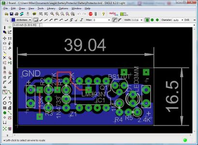
So the board should be designed like you want it. See first picture
Basically, I try to make my PCB as small as possible with as few vias and jumper wires as possible.
Comments: The big white rectangle is the board outline, dimensions in mm are shown. This is helpful to make sure it’s printed out to the correct size.
Component outlines and designations are in white.
The blue is the traces that will be the copper(bottom).
The round green holes are where components will be inserted.
The square green holes are the vias.
The red lines are the traces on layer 1. They will be wires soldered to the vias.
For most of my resistors and diodes, I used vertical components.
For R5, I changed it to horizontal orientation so that it routed easily.
The wide blue areas are the polygon on the ‘Gnd’ net.
Step 3: Toner Transfer Process


The board information needs to be transferred to the physical PCB. I use something called toner transfer using a laser printer. An ink jet printer will not work for this process. Glossy paper is also required. I bought some glossy paper but it didn’t work very well. So I use some glossy paper from glossy magazines. Pages need to be shiny and thinner is better.
Now, I create the images for printing on glossy paper.
The board view in Eagle Cadsoft contains a lot of information that you don’t want on the actual PCB. Here’s how you limit that information.
Bottom trace Layer
Eagle: In the board editor, there is a little icon called Display (Show/Hide Layers). It's in the upper left corner. Click on it, select <None> then click on (highlight) these layers:
16-Bottom
17-Pads
18-Vias
20-Dimensions
Now, just the bottom trace layer should be displayed. See first picture
Select <File><Export><Image>
<Monochrome>
600 DPI.
<Browse> Select the directory and file name, e.g, AudioTraces.png that you want.
Click <OK> to export as image.
See first picture.
Okay, now the file is exported as a PNG but I like to use JPEG files. So what I do is find the PNG file, right click the mouse on it, select <Open with><Paint>
In Paint, select <File><Save as>, select <jpeg>.
Note that the traces(copper) are in white. For toner transfer, they need to be in black. So you need to transform it. Now I have Adobe PhotoShop Elements. There are other programs that can do this. I know some people use the free GIMP program. But here’s how I do it.
Make Negative:
Open jpeg Image with PhotoShopElements
Select <Image><Crop> Crop <Check>Limit to just the rectangular outline
<Select> All
<Filter><Adjustments><Invert> Now you will have black traces on white background, see picture.
<File><SaveAs>....
e.g., AudioTracesINV.jpg. Now you have the inverted image.
Touchup: If you want to make any touchups, I use Paint.
Now this file could actually be used. But most printers print an 8.5” x 11” page, so a lot of the page would be wasted. So I make multiple copies to put on a single sheet. Each PCB requires one image, so I can make multiple PCBs from one sheet.
Make multiple copies:
Open the inverted image with Photoshop Elements
Create a new base file, <File><New> Width 8, Height 10.6 Resolution 600 pixels
To view both images, select <Arrange> (Select the grid) so that the display will show both files
Click on the Inverted image, <Select><All> <Edit><Copy>
Click on the base file, <Edit><Paste> The inverted image will be copied to the blank
Use Mouse to select Move tool, move the image to upper left corner
<Ctrl-V> to repeat pastes. For my small PCBs, I usually make 6 or 8 images.
Leave space around the edges as my glossy paper is less than 8.5 x 11.
Then save it. <File><Save as> , e.g., AudioTracesMulti.jpg
I use MS Office Picture Manager to print
Print a sample on regular paper, don't forget to unclick "Fit to Page". This is critical to keep the printout the correct size.
If it is not the correct size, figure out the difference. I had one that was 5% to small. So in MS Office Print Manager when you're getting ready to print:
Select <Options>, Printer Properties, <Paper> <Scaling Options> 105 <Percent> <OK>
To summarize: the Eagle Cadsoft trace image needs to be converted to a 'negative' (white is black and black is white) You need to find a program and method to do this. I also put six to eight copies of this on a page so the printer will print out multiple copies on a sheet of paper.
Glossy printing:
Here is the setup I used for my Laser printer. This process will not work with an ink jet printer. The idea is that you want it as black as possible and no scaling.
Samsung ML-1865W Setup
Basic: Quality: Best
Paper: Scaling Options: 100%
Graphics: Darken Text, All Text Black
Fine Edge
Toner Saver: Off
Darkness: Dark
I had better luck with glossy magazines like Woman's Day. My printer isn’t a flatbed and the glossy paper was too flimsy to run through it by itself, so I took a sheet from the magazine and taped it to a regular piece of paper. It's better to use a page that's mostly white so it's easier to see where your image is on the glossy. See picture. Here one of the glossy images is already removed and cut up, but I had taped the bottom and the top before printing.
Stick this in the printer paper holder(in my case, gloss side up) and print.
Touchup: If any touchup is needed, use a Sharpie.
Step 4: Silk Layer


Since we’re doing printer stuff, I also made a silk screen. This is all the component outlines, designations and values to make it a little easier to put components in the right spots.
So we have to create an image for the silk screen.
Eagle: In the board editor, there is a little icon called Display (Show/Hide Layers). Click on it, select <None> then click on these layers:
17-Pads
18-Vias
20-Dimensions
21-tPlace
25-tNames
27-tValues
Now, just the silk screen and pads should be displayed.
Select <File><Export><Image>
<Monochrome>
600 DPI.
<Browse> Select the directory and file name that you want,e.g., AudioSilk
Click <OK> to export as image.
See picture. As before, I use Paint to convert it from a PNG to a JPEG file. Again you will notice that the stuff you want printed is in white and needs to be black so again we need to Invert. So what isn’t so obvious is that since the silk screen goes on the opposite side of the traces we need to flip the picture. Here’s my procedure.
Make Invert and Flip:
Open Image with PhotoShopElements
<Image><Crop> Crop <Check> Crop it so there's not a lot of wasted space
<Select> All
<Filter><Adjustments><Invert> Make traces black instead of white.
<Image><Rotate><Flip Horizontal Makes a mirror image
<File><SaveAs>....
See picture. Some of you may notice that this is not the same board. You are correct. Like the traces, I made multiple copies on a page.
Make multiple copies:
Open the inverted image with Photoshop Elements
Create a new base file, <File><New> Width 8, Height 10.6 Resolution 600 pixels
Click on the Inverted Silk image, <Select><All> <Edit><Copy>
Select base file, <Edit><Paste>
Use Mouse to select Move tool, move the image to upper left corner
<Ctrl-V> to repeat pastes
Print sample, don't forget to unclick "Fit to Page"
Use the same procedure to print on a glossy page. I guess I don't have a picture of this.
Step 5: Etching on Top Layer


So I was making a shield for an Arduino. See picture. Shields require header pins that extend below the PCB but the components are usually on top. This is a problem for single sided PCBs. If you put the traces on the bottom, the components will solder normally but what about the headers? Will one option is to insert the headers but not all the way flush so that there is a space between the header insulator and the PCB. Thus, you can solder the header pins in there.
For this shield I decided on a different method by putting the traces on the top side. This makes it easy to solder the headers but the components have to be soldered on the top side. This is fairly easy for resistors, capacitors and wires such as my shield circuit. It is harder for IC sockets and header pins. You have to decide which way is best for you.
Procedure:
In Eagle boards, when you do Autorouting, select TOP is - and Bottom is N/A. This is opposite of the previous method.
Save traces, the same way as above. The traces will be red.
Save image as above.
But when you convert the image, you must Invert and Flip (Horizontal) like you do with the Silk.
Silk: Warning: Do not try to put the silk screen on the side with the traces. I tried it and had the following problems. One. it silked the pads so you would have a hard time soldering to them. Two, the copper traces are slightly thicker than the raw board so the silking will have a harder time getting to the raw board.
If you put the silk layer on the bottom, then you Invert but do not flip. Or you can do without a silk which is what I will do.
To summarize: the trace layer is made like the silk and the silk is made like the trace.
Step 6: Printed Circuit Boards (PCBs)


I bought my blank PCBs on ebay of course. It is single-side (copper on one side only). See picture
Cutting PCBs: There are a lot of Internet ideas about cutting PCBs. I like to use a steel ruler.
See pictures. I like to mark and score both sides, then carefully bend the sides until it breaks apart. As you can see, I didn’t do a very good job of aligning my score marks.
*********************************WARNING********************************************************
When using acetone, you should always wear gloves and use in a ventilated area.
*********************************WARNING********************************************************
Cleaning PCB copper:
Scrub with Scotchbrite
Wipe with acetone on a paper towel
Once cleaned do not touch copper surface
Attaching the traces glossy:
I cut the glossy outline slightly bigger than the PCB so I have something to tape to, lay it down with the black traces up.
Lay the cut PCB over it with the copper side down.
Align the PCB over the outline.
Tape the PCB to the glossy paper so it won’t move.
See picture. The bottom shows what a bad job I did cutting the PCB but it’s big enough for all of the traces.
Next you want to transfer the outline to the PCB.
Toner Transfer:
Turn clothes iron to hottest setting. See picture.
Wait until iron is hot
Place PCB on flat hard surface with glossy paper sticking up. I used the sink counter in
my bathroom.
Place and press iron on paper/PCB
Leave it on for about 30 seconds
Using tip of iron, press all around PCB several times
If you used glossy magazine, you should start to see traces peaking through
See picture
Iron some more
It's probably pretty hot at this time so be careful.
Remove the tape (I used my utility knife to trim the paper to the PCB shape,
then removed the tape from the PCB)
Soak in water and scrub with an old toothbrush
The paper should come off leaving black traces on the PCB
NOTE: IF there is a problem with the traces, you can scrub the traces off with Acetone and repeat the process since you made multiple copies, right?
See picture. You can make touchups with a Sharpie. For this PCB I had to make some of the transfer larger as the connector I was using had flat pins instead of round ones and I couldn’t figure out how to do that in Eagle Cadsoft so I did it on the unetched PCB.
Step 7: PCB Etching

Etching is the process of removing the copper from where you don’t want it. The principle for toner transfer is that the laser ink outlines the traces you want. The etchant will remove copper except where there are laser ink traces, then the Acetone removes the laser ink.
I use the follow etchant per this Instructable:
https://www.instructables.com/id/Stop-using-Ferric-Chloride-etchant!--A-better-etc/
*********************************WARNINGS***************************
The muriatic acid is hazardous. Do not breathe the fumes
Do this outdoors or in a ventilated area
Use plastic bottles, containers and utensils. NO METAL!
Pour the hydrogen peroxide in first
RULE: Always Add Acid (AAA) Then add the muriatic acid
*********************************WARNINGS***************************
Two parts hydrogen peroxide (3%)
One part Muriatic acid (31%)
Etching:
Mix etchant in a plastic container large enough to hold the PCB
Place PCB in container
I guess it helps to stir up solution
Wait until copper is etched away from between traces. This may take 30 minutes.
NOTE: The Instructable says you can use this etchant over and over. I haven’t had any luck doing that. Do not throw old etchant away or flush it. Recycle as hazardous waste.
Now you have an etched PCB with black traces. Using a funnel, pour the etchant into a plastic bottle with a lid.
Wash the container and the PCB with water.
Put some Acetone on a paper towel and clean off the black toner.
See next picture. This is an etched and cleaned PCB.
Step 8: Drilling PCB and Silk Screening


Next I drill the PCB. Some people like to use a drill press. I just use my Harbor Freight Drill Master.
For drill bits, I bought some 0.8mm bits on ebay and some 1.5mm. For most holes, I use the 0.8mm. See pictures.
So all of the little copper circles need to be drilled for components. Place the PCB copper side up over a piece of scrap wood or fiberboard.
My little Drill Master with the ebay drill bit is not very steady. When turned on the drill bit tip warbles. What I do is probably a bad way to do it but I have the Drill Master off, put the drill bit touching the copper, then start the Drill Master and drill the hole.
TIP: Since I am a little anal about using up old drill bits first, I have a method of identifying old and new. My containers contain about 10 drill bits. I put the new ones in with the tip sticking up and the used one in with the tip sticking down.
Silk Screen:
An advantage of drilling the holes first, is when you lay the PCB over the glossy paper silk screen, you can line up the holes.
One method I used is to punch four holes through pads near the corners of the PCB in the silk screen glossy.
Stick some resistor leads in the corresponding four holes of the PCB. See picture.
Slip the silk layer glossy onto the resistor lead and place the glossy flush with the PCB. See picture. This aligns the silk layer with the traces and pads.
Tape the PCB to the silk glossy, remove resistors and iron as with trace glossy.
Use same procedure, remove tape, soak in water and scrub with toothbrush to remove glossy. You should have a silk screened PCB.See picture.
Process is the same. Align the PCB over the silk screen. Tape the PCB to the glossy. Iron away.
Remove tape, soak and remove paper.
NOTE: IF there is a problem with the silk, you can scrub the traces off with Acetone and repeat the process.
Step 9: Finish PCB


Now you can solder in wire jumpers and components.
Tips: Raw copper is hard to solder. If a PCB has been sitting around for a long time, it may oxidize, so a light scrubbing with Acetone should help. I usually forget to do this, however.
Some homebrewers, apply something called liquid tin to the copper. I don’t. It’s expensive.
See first picture. The copper side shows a cut and jumper. This is what happens when you don’t thoroughly check your schematic and parts. This was caused by a custom part I made not quite correctly.
See next picture. The component side shows one of my wire jumpers in vias. The copper wire to the right is just a ground connection I added for troubleshooting.
The last picture shows my Arduino weather shield.
Finished! Test it!

Participated in the
Hurricane Lasers Contest


