Introduction: SMD Nixie Clock


Background:
I initially wanted to build something because I was looking for a project to do, and finally wanted to do a project with SMD components. The considerably smaller size of the SMD components would allow me to make smaller PCBs, and open up the world of SMD components to me for future designs. I had built a word clock several years back following an Instructable, and thought that another clock would be fun (and give me an opportunity to give something back to the community). It would also have the benefit of being slightly useful after building it. Nixie tubes also just look reallynice.
There were many bumps along the way, and I learned a lot about using these small SMD components and reading the datasheet (did I say read the datasheet!).
Follow along and I will show you how you can build one of your own!
Below is a quick video of what the clock will look like. (The word clock is in the back!)
Step 1: Gather Materials


To build this clock, you will need the following:
Materials:
6x IN-14 Nixie Tubes
2x IN-3 Nixie Indicator Bulbs (they come in a pack of 10)
1x ATMega328P Microcontroller
2x HV5622 High Voltage Shift Register
1x 78L05 5 V Voltage Regulator
1x DS3231 Real Time Clock
1x CR2032 Battery Holder and Battery
2x 4.7K Resistors
2x 120K Resistors
6x 27K Resistors
1x 10K Resistor
60x Machine-tooled Female Headers
1x Main PCB (see next step)
3x Right Angle Push Buttons (I had some on hand; I didn't remember where I got them from.)
1x Barrel Jack Connector
1x 12 V Barrel Jack Power Supply
Wires with female headers on the end
4x 4-40 Screws
4x 4-40 Nuts
Some wood
Tools:
Soldering Iron
Flux
Flush Cutters
Needle-nose Pliers
Isopropyl Alcohol
AVRISP Programmer
Saw
Router
Drill
Optional: CNC Mill / Laser cutter / 3D Printer etc. (if you have access to one)
I ordered some of the electronics components from Mouser, and the rest I had on hand (can also be ordered from Mouser, Digikey, or your other favorite part distributor). The PCB was fabricated by OSHPark. The power supply board and Nixie tubes were from eBay.
Step 2: Designing PCB


Prior to this project, the last time I had designed a PCB and had it made was over two years ago. And that time I was using Eagle for PCB design and only through-hole components. This board was going to have a much tighter fit and SMD components (along with some through-hole parts). Also, I had to learn how to use KiCAD because the free version of Eagle doesn't supports boards larger than 4" x 3.2".
The circuit uses an ATmega328P for the brains, and two HV5622 high voltage shift registers prove the necessary control lines to independently control each tube's digits without multiplexing. A DS3231 RTC provides the accurate timing, and three buttons allow for user configuration. Several passives are used for pull-up resistors on the I2C lines, current-limiting resistors for the Nixie tubes, and filtering capacitors.
You will first need to layout the schematic for the entire circuit. Don't kill me for the horrendous layout; I know mine is a little messy (as I wasn't sure how to go about making multi-sheet schematics) and you can definitely improve on it.
I have no idea how to "properly" layout PCBs, and if any of you have any suggestions, I would be more than happy to get some feedback. I think for now it will get the job done since the signals are only digital and not high speed. (I would recommend redoing the layout for this board, especially with regards to the high voltage sections, to ensure sufficient clearance between other wires.)
I designed this board to be the same width as the high voltage boost converter board so it will fit into a box nicely at the end. You can buy the PCBs from OSHPark. I know this seems a little counter-intuitive to DIY, but I simply didn't have the materials to make my own at home. The price also seems a little high, but remember that OSHPark sells PCBs in batches of three. If you order from them, you can make three clocks!
However, the KiCAD files are also available on GitHub and in a zip below. Feel free to modify them or use them to etch your own PCBs at home.
There are some issues with the PCB that I go over in the next section, but they weren't too bad. (Without rapid prototyping capabilities, the long wait time time and relatively high costs between prototypes can seriously slow down development. Luckily, my PCB's could be fixed with simple adjustments.)
I didn't design the high voltage boost converter (but I am learning!) and ordered it from eBay. It will connect into the main PCB and supply it the necessary voltage for running the Nixie Tubes.
A week later, the package from OSHPark arrived. I finally had something physical, and could begin assembling the clock.
I immediately discover the errors in the PCB during the next step, the soldering process.
Lessons learned: Measure twice, cut once. Pay attention when you only have one shot at getting something right (and keep it looking nice).

Step 3: Soldering and Setting Up the HV Booster


This was the step I was looking forward to the most. I was finally going to be able to solder SMD parts for the first time, which is the reason why this design can be this small. (Actually, I had gotten a little practice by buying one of those SMD practice kits from eBay.) Pay attention to which corner of the ICs have pin number one (denoted by a small circle), and line them up the number "1" I put on the silkscreen. You'll have a bad time if you solder the chip on in the wrong orientation. The DS3231 lines up with a notch. Solder down pins on opposite corners to first get alignment right, then do the rest.
Also, all the errors I made with the PCB suddenly became very obvious in this step. I've numbered all the mistakes it has, so you'll be able to make the same fixes I did when assembling the board.
You'll first want to break open the socket pin rows and extract the actual metal pins. It turns out that they make really good sockets for Nixie Tubes, allowing you swap a tube out if one should ever go bad on you in the future. I used a the flush cutters to break apart the pins. (0) The pins can be somewhat of tight fit in the holes, and you may need to use a little bit of force.
(1) It turns out the package outlines I used that were already in KiCAD didn't exactly match the outlines of the components. (I should have really checked this before.) The HV5622's had longer legs than normal, and I could safely trim off some of the leg and still get the IC to fit in the footprint. This isn't good practice, but this bodge got the job done.
(2) Another problem was that I hadn't considered which way the digit separating lamps (the small IN-3s) were going to face. I assumed they would be omnidirectional light sources, but just like the numerical tubes, they have a rear metal shield. Luckily, I was able to simply switch the position of the current-limiting resistor and the tube to flip the orientation of the tube. Also, pay close attention to the polarity of the small IN-3 tubes. There should be a small arrow at the base of the tube pointing in the direction of conventional current flow (+ to -).
During this process, flux is your friend. It will make SMD soldering much easier and make the solder create a nice joint to metal. If you use too much solder, solder wick is your next best friend.
The 10K resistor is the pull-up resistor for the reset pin by the ATMega328. The 4.7K resistors by the the RTC are pull ups for the I2C bus. The 120K resistors limit the current of the small IN-3 bulbs, and the remaining 27K resistors limit the current of the main numerical IN-14 Nixie tubes.
And please be sure you are using the right type of flux. I had some "flux" lying around that I never had any use for, and after I had used it, I found out it was for pipe welding and was highly corrosive. Well then. It worked, but it was likely the cause of the plague of issues I ran into afterwards.
Before testing out all the circuitry, we need to setup the high voltage boost converter. We want to run the tubes at the lowest voltage possible while still being able to light up every digit completely. With the 27K resistor in parallel with the digit, I did some simple measurements while slowly upping the voltage until each digit could light up completely. In the end, you will need to set the voltage to around 160 V. We will adjust this more later.
CAUTION: BE CAREFUL WHEN DEALING WITH HIGH VOLTAGES
I'm not joking.
Step 4: Cleaning Up and Connecting All Other Components


Now get out your vintage Nixie tubes, along with small needle-nose pliers, and begin straightening out all the legs. Make sure they all point downwards and are parallel to each other. Hold them about the sockets on the PCB or even test fit them to make sure you get the right spacing for all the legs to fit in nicely. Keep all the tubes unplugged when you are done.
Be patient. I know this will be frustrating when that one leg won't enter the socket, but trust me. You don't want to have a leg break from repeated bending.
With all the legs nice and parallel. and try to trim them all to the same length, while keeping as much of the legs as possible.
After all the small components have been put on the PCB, it's time to clean up all the flux. This wasn't an issue I had initially considered, and flux turned out to cause a plethora of issues. I had written up some simple code to cycle the Nixie Tubes, but nothing was working. Every digit just remained on, and every once in a while the clock would cycle a couple of digits before flickering and going back to turning all the digits back on. I was stumped. I was getting slightly frustrated, and after mangling my code for an hour and poking around in the datasheets I thought I found the problem.
The HV5622 datasheet stated that the recommended logic supply voltage should be around 12 V. Uh oh. I was now pretty frustrated, yet disappointed that I didn't see this earlier. But the fact that the cycling worked for a bit gave me hope that a 5 V logic supply would work.
I noticed the flux residue on the PCB I thought that the flux might be conductive. A little bit of Googling turned up that most types for electronics (which I already got wrong) shouldn't be conductive, but people still clean it off. The 170 V for the Nixie Tubes probably don't help. I got out some cotton swabs, an unused toothbrush, and isopropyl alcohol, and began scrubbing.
Be sure to work in a well-ventilated area. The fumes from the alcohol are not good for you. I also assume you worked in a similar location for soldering, right?
After several cycles of testing and cleaning, I got rid of all the unwanted connections. It was extremely satisfying to not see the "1, 2, 3, and 4" digits light up when I only toggled the "3" digit.
I felt pretty lucky that everything worked out and the high voltage didn't cause something to release the magic smoke.
Try not to test too often, as you will put additional stress on the Nixie Tube legs from the repeated insertions and removal during testing. You may want to jump ahead to the next step for a bit and come back to get a program running on the clock for easier testing. Use a multimeter to test for unwanted connectivity.
Moral of the story: Use the right flux, read the datasheet completely, and clean your PCBs.
Step 5: Programming


Now with the hardware issues out of the way, programming could go full steam ahead. I programmed the clock with C in AVR Studio. The code is rather simple, and can be broken up into three modules. One module handles all the initialization of the clock. The second block manages all the button inputs and their states, and the last module keeps track of the clock's state. If you want to make you changes to the code, there is a simple function I created, called writeOut, that makes it easy to output whatever you want to the clock's display. All you need to do is set the individual values of an six element array to their corresponding digits, and pass that into the function.
Compile the code using AVR Studio, or from the command line with avr-gcc, and upload the code using an AVRISP connected to the programming header in the middle of the clock.
I used the Timer library and DS3231 library to get the code working quickly.
The clock currently has four main functions: time (default mode), date, temperature, and timer. The time and date functions, as their name implies, tells the set time and date. The temperature mode uses the temperature sensor in the RTC to tell the temperature in degrees Celsius to the nearest quarter degree. The timer mode allows you to start and stop a timer (which is currently not very accurate because it only uses the ATmega's internal oscillator. After 10 seconds of inactivity in any mode other than time and timer, the clock goes back to telling the time.
In time mode, every minute, the clock does a cycling animation to prevent cathode poisoning in the Nixie tubes. The animation is visible in the video at the beginning of the Instructable. Be sure to switch back to the clock manually if you used the timer mode and are done with it.
The base code is available on my GitHub: https://github.com/njeff/nixie-clock. Have fun making changes to the code or improving the current one.
Step 6: Debugging


After the code is running on the clock, make sure all the functions are working. You may want to adjust the voltage of the HV booster since all Nixie tubes are made slightly differently and some digits may not be fully lit.
Also, if anyone comes across any bugs in the code let me know so I can fix them.
Feel free to make adjustments to the code so everything is to your liking.
Once again, be careful when working with high voltages.
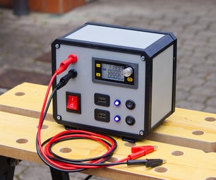
Step 7: Building Case


This clock part is essentially done, but it looks rather bare. It's a little odd to have the high voltage power supply dangling off to the side. Also, you may hear an annoying buzzing sound from the switching boost converter, and it's probably going to piss you off rather quickly. To deaden that sound and make this look much snazzier, we are going to make a nice case for the whole thing. There's a reason why the main PCB is the same width as the power supply.
(I'm going to be honest I didn't get around to making a case yet, and I sort of wrote this next part in preparation for it and never got it done. So anything afterwards is just what I intend to do. I just haven't found the time for it and wanted to publish this after sitting on it for nearly half a year. :) The main circuit is complete, and what you do for the case is up to you!)
Update: I made the case (finally!).
You can use a CNC mill, a laser cutter, a 3D printer, a water jet, or a stone, or give it a more human touch by making the case by hand. Whatever you happen to have. I built a DIY CNC mill that's rather un-rigid (but still better than my hands) and used that to make part of the case for my clock. I know that not everyone has access to one, but you can build a perfectly nice case with more common hand tools. If you do want to use one, check to see if you have nearby maker spaces or "tech shops." Besides, my CNC can't even cut perfect interior right angles (or any interior angles for that matter), and the setup time is rather long. Not to mention the CNC generates a relatively large amount of dust and noise for simple profile cutting.
I used a piece of scrap wood I bought at a nearby lumber store.
Be sure to remeasure the size of the PCB, as it can differ slightly from the intended lengths in the digital design. Better to make the pocket for the board larger than smaller.
To make the cover of the case, measure out how much space the tubes take up above the main PCB and draw some guide lines on the cover material. You can use the measurements from the PCB files, but be sure to remember the tubes are larger than their footprint.
Line up the power supply PCB with the pocket in the case, and mark where the mounting holes should go. Then line up the main PCB and mark out where its mounting holes should go. Drill the holes, but don't pass all the way through.
With the main PCB in place, mark out the position of the buttons. Remove everything and drill out the holes.
Mark where you want the barrel jack will to appear, and drill out a hole for that too.
Feel free to let your creativity run wild and create a design you like.
Step 8: Final Assembly
With a case in one hand, and the clock in another, bash them together to make the finished product.
I'm joking. Test fit all the components to make sure the height of the main PCB is high enough to clean the power supply and barrel jack.
Begin mounting all the electronics, starting with the HV power supply and the barrel jack. Screw in the power supply and glue down the jack. Afterwards, screw in the main board.
Finally, slip the top cover around the Nixie Tubes and mount it with screws or glue, depending on how you want it to look. I recommend screws for easy disassembly.
Step 9: Conclusions

You're done! After all your pouring out all your blood, sweat, and tears (none of which are guaranteed), you are finished. Now you have a fully functional Nixie Tube clock!
If I were to make this project again, I would definitely fix up the errors on the PCB, and try to move all the passives to SMD. I had the through hole passives on hand already, and wanted to use them up. Also, I would move the power supply on the same board as the rest of the circuit. This would give me an opportunity to learn about analog power supply design, and I would probably have to pay more attention to layout. It would also make the overall design cleaner.
Feel free to modify the code to add more functions and animations. Make another case. Heck, get different Nixie tubes and create a completely new design. But in the end, have fun! I hope you enjoyed reading this and learned something along the way. Keep on making!

Fourth Prize in the
Circuits Contest 2016