

Introduction: Transistors


The humble transistor is the building block of all digital electronics. By creating different configurations of transistors (in relation to other electronic components), you can create circuits which provide the groundwork of binary logic. This is the basis for all modern computing and has helped us do important things like post pictures of cats on the internet, and put astronauts in space.
Transistors also do some interesting things in the analog world as well. They are also responsible for guitar effects pedals and helped David Bowie put everyone in space. Throughout this lesson, we are going to largely be looking at transistors in their simplest analog sense.
Step 1: What Is a Transistor?


A transistor is an electronic component that takes a small amount of current and amplifies it.
Unlike all of the other components we have looked at where electricity goes in one side and out the other, a more complicated process is at work within the transistor.

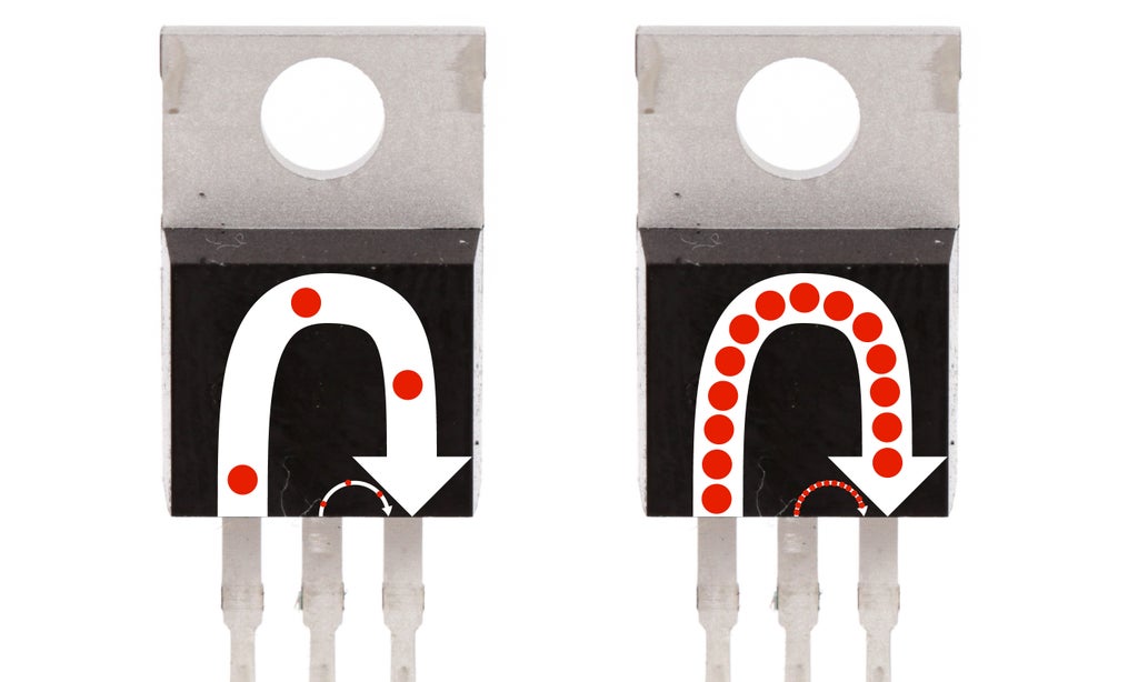
A common transistor has three pins which are the base, collector, and emitter. Since transistors come in all different shapes and sizes, and the pins are rarely marked, you will need to look up which pin is which. If you image search for "[INSERT TRANSISTOR NAME] pin diagram" you will quickly find out this information. For instance, let's find out the pin diagram for a 2N2222 transistor by searching for "2N2222 pin diagram." Easy-peasy.

In a schematic a transistor will be represented as an NPN, which has the arrow pointing outwards away from the vertical line, or as a PNP, which has the arrow pointing inwards towards the line.
Step 2: NPN Vs. PNP

There are two types of basic transistors in this world - those which are NPN, and those which are PNP.

To better understand the difference between the two, let us revisit diodes for a moment. Like diodes, transistors are made up of configurations of PN junctions.

You could hypothetically say that an NPN transistor is basically 2 diodes back to back. In a theoretical world, you would be right, but in the real world you can't really say that at all. The difference being that not only are the P-regions in a diode considerably bigger, they are also not actually being directly connected. Each P-region is actually being connected to a wire lead, which in turn behaves neither like a P-region or an N-region as far as electrons are considered. This demonstration is more like an NP-WIRE-PN junction. This is clearly not the same at all. However, this idea of a PN bias is important to consider.

Unlike a diode, an NPN transistor has a very thin P-region - no wider than a couple of wavelengths of light - sandwiched between two N-regions. When a current is applied to the P-region (connected to the base pin), it forward biases the base and collector pins, effectively shrinking the depletion zone on both side of the P-region in relation to the current being applied.

This forward bias arrangement between the base and emitter allows electrons to flow from the base pin to the N-region connected to the emitter (like a diode). Presuming that the electrical signal at the collector is also more positive than the one at the emitter, the electrons at the collector are able to take a free ride through the activated P-region to the emitter. Put another way, the current passing from the base to the emitter works like a Trojan Horse to activate the P-region and allow the much larger current hanging out at the collector to pass through the P-region to the emitter.
When a small electrical current is applied at its base pin, it amplifies it such that a much larger current can pass between its collector and emitter pins. The amount of current that passes between the collector and emitter pins is proportional to the current being applied at the base pin.

A PNP transistor on the other hand, works opposite of an NPN transistor. It has two P-regions and a very small N-region in the middle. On account of this it is reverse biased between the base and emitter. Thus, when a current is applied, this reverse bias works like a diode and stops electricity from flowing. It is only when the current begins to be removed from the base that electrons can pass freely between the collector and emitter.
Basically, an NPN transistor allows electricity to flow when a current is applied to its base and stops the flow of electricity when it is removed. It can let varying amounts of electricity pass through in a direct relationship to the current on its base pin.
Notice when the button connected to the base pin is pressed, the LED turns on. This is because the buttons is connecting the base to power. When the button is not pressed, the 10K resistors is connecting it to ground. This type of resistor configuration is called a "pull-down resistor" because it keeps the pin grounded when not in use.
If you were to replace the buttons with a variable resistor, you would be able to vary the brightness of the LED wired to the transistor.
A PNP transistors does the exact opposite of this. When the button is pressed, voltage is applied to the base pin and the LED is turned off. It can also be dimmed using a variable resistor.
Step 3: Power Ratings

The transistors with the highest current rating typically have metal plates in the back connected to the collector pin. It is attached to this pin in particular because the most amount of energy passes through it. These plates dissipate heat and have a hole for attaching the transistor to a heat sink.
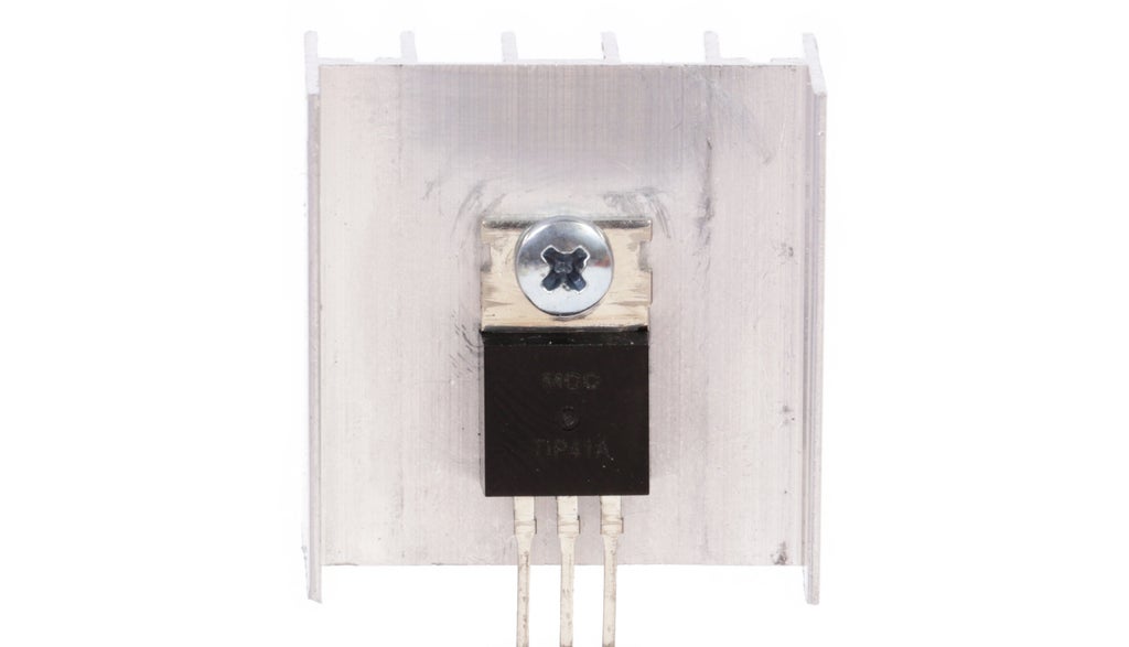
A heat sink is a piece of metal (typically aluminum) that has been shaped in such a way to maximize its amount of surface area. Basically, it has a bunch of little fins which allows air to circulate around the part and cool it down. The transistor is bolted to the heat sink to transfer the heat outwards and cool off. This prevents the transistor from overheating and malfunctioning.

Additionally, to maximize heat transfer between the transistor and the heat sink, thermal paste can be used. Apply a thin coat between the transistor and heatsink before bolting them together.


