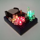
Introduction: 3P4W LED Clock With Temperature Display


This is a simple clock project based on ti MSP430G2231. The MSP430G2231 micro-controller comes included in the $4.30 TI Launchpad kit. The project objective is to create a working clock with minimal components. In order to achieve this objective, current limiting resistors for the LED display were omitted. also multiplexing is used to reduce the io pins needed to drive the LED display.
For a 4 digit x 7 segment display we need to drive 32 LEDs (including the decimal dot). the MSP430G2231 has only 10 IO pins at most, so instead of driving individual LEDs we use multiplexing to briefly turn on and off led segments for each digit. We do this ever so quickly to fool our eyes that the LEDs are constantly on. This is also known as POV (persistence of vision). The control (user interface) is also arranged so that we only use one tactile button for input. The firmware capture long button presses (press and hold) for menu rotation and normal button presses for menu selection.
Another objective of this project is to lower the admission level for anyone who is thinking about picking up electronics as a hobby. No special tools are needed to built this project. DIP components are used instead of SMD so no special placement tools are needed. Breadboard is used instead of PCB to eliminate the need of access to a soldering iron. Cost of components are minimal (the micro-controller programmer is included) and parts are commonly accessible.
I called this the 3P4W clock as it takes only 3 parts (alarm is optional) and 4 wires to assemble this project.
TI LaunchPad Link: http://processors.wiki.ti.com/index.php/MSP430_LaunchPad_%28MSP-EXP430G2%29?DCMP=launchpad&HQS=Other+PR+launchpadwiki-pr
Below is video on full construction, direct link if embedded doesn't work
http://www.youtube.com/watch?v=Ama9BEEP9gs
Step 1: Features and Parts

Features
. Minimal components, 3 parts (4 parts if you need alarm)
. 4 jumper wires on a mini breadboard
. Battery operated from 3V
. Use of internal VLO clock (~12Khz) to keep time, sleep mode takes less than 1uA power
. VLO is calibrated against DCO at startup, DCO in turn use factory calibrated value
. Manual calibration allow fine adjustment to oscillator timing
. Fairly accurate if you consider that there is no crystal used
. Ambient temperature read in metric and imperial units
. Optional alarm if you connects a buzzer (auto-detect), this will make the 4p4w clock
. Hidden easter egg function for you to find
Parts
. MSP430G2231 (from your Launchpad kit)
. 4 digit 7 segment LED display (red works best on 3V power)
. Tactile button
. Buzzer 3V (Optional, and becomes the 4P4W clock)
You will also need a breadboard to place your components, a 3v 2xAAA battery holder with batteries and 4 connecting jumper wires, I used a 170 tie-point mini breadboard as the platform and used network cable cores as jumper wires.
The LED display is commonly available in ebay, look for those 0.4" or 0.36" 4 digit displays, you will want to make sure it's common cathode and the pin layout matches (most do)
   __a__      (0) A  F (1)(2) B
 f|     |b    -+--+--+--+--+--+-
  |__g__|     |                |
 e|     |c    |Pin1            |
  |__d__|     -+--+--+--+--+--+-
                E  D  . C  G (3)
Tools
. Computer with either Linux or Windows
. TI LaucnPad, EZ430-F2013 Kit, or other MSP430 programmer
. mspdebug or TI CCS development environment (programming software)
Step 2: Breadboard Layout and Assembly


. Cut to length 4 swg#22 wires (4W) and insert into breadboard as layout diagram shows.
. You may use other wires, I used core wires extracted from common network cables.
. Insert MCU (1P) into breadboard as per layout diagram.
. Insert LED display (2P), note that lower row of pins share the same holes w/ MCU.
. Insert tactile switch (3P) and optionally the 3V buzzer (4P).
. Schematic diagram also attached for references.
You can also watch the video on the first page, which shows complete assembly and firmware uploading plus operation procedures, all within 3 minutes.
Step 3: Flashing the Firmware


The firmware is the actual binary instructions that the MCU executes and is the brain of the 3P4W clock.
Programming Hardware Tool Setup
In this step you will need to flash / program the MCU. You will need a programmer to do this. You can either use the TI LaunchPad or the TI EZ430 dongle as a programmer. In either case the basic idea is to;
. Identify the power supply (Vcc and Gnd) points in your programmer.
. Connect them via jumper wire to pin 1 (Vcc) and pin 14 (Gnd) to the MCU.
. Identify the SBW (spy-by-wire) ponts (Data and Clock) in your programmer.
. Connect them to pin 10 (Data) and pin 11 (Clock).
link to LaunchPad:
http://processors.wiki.ti.com/index.php/MSP430_LaunchPad_%28MSP-EXP430G2%29?DCMP=launchpad&HQS=Other+PR+launchpadwiki-pr
link to EZ430:
http://focus.ti.com/docs/toolsw/folders/print/ez430-f2013.html
Programming Software Tool Setup
I had used mspdebug:http://mspdebug.sourceforge.net to download the MCU firmware. See link for instruction to download and build mspdebug.
if you are using the RF2500 kit or the launchpad as your programmer, use the following commandmspdebug rf2500 "prog 3p4w-clock.elf"
if you are using the EZ430 kit as a programmer, use the following commandmspdebug -d /dev/ttyUSB0 uif "prog 3p4w-clock.elf"
It is also possible to program the MCU under Windows via the TI's integrated development environment CCS. CCS can be downloaded from TI's website:http://focus.ti.com/docs/toolsw/folders/print/ccstudio.html
Firmware Binaries
Both 3p4w-clock.elf and 3p4w-clock.txt can be obtained here
3p4w-clock.,elf for Linux:
http://sites.google.com/a/simpleavr.com/simpleavr/msp430-projects/3p4w-clock/3p4w-clock.elf
3p4w-clock.,elf for Windows:
http://sites.google.com/a/simpleavr.com/simpleavr/msp430-projects/3p4w-clock/3p4w-clock.txt
Step 4: Uncover the Hidden Easter Egg

Clock Operation
- if buzzer is connected, firmware allows for alarm setting and usage
- single button press toggles thru hours + minutes, alarm on/off + seconds, and sleep modes
- long press enters setup mode, subsequent long press rotates thru menu
- menu items cycles thru SEt, ALr, Cnt, AdJ, bri
- in 'SEt' time setup mode, short press enters setup
- once in setup, short press toggle digit values (hours, minutes) and long press confirms
- choice of 12H or 24H display
- likewise in 'ALr' alarm setup mode, hours and minutes can be entered
- choice of alarm On or oFF
- 'Cnt' selects the kitchen timer function, enter minutes and seconds, long press to confirm and starts count down
- in 'AdJ' calibration setup mode, 0-60 'gain value' can be setup to make clock faster, each unit adds about 0.5% to clock speed
- when in sleep mode, MCU goes in power down mode, consuming less than 1uA of power, watchdog timer is set so that system wakes-up every 1/8 second. this, however makes the time keeping to be always slow as it takes a few cycles to power up the MCU again. therefore we must have a calibration value to keep accurately
- last setup values saved in EEPROM and will be used for the next power up
- in 'bri' dimmer setting, short presses cycles through available brightness levels, long press confirms setting
- led segment multiplexing includes time delays to compensate for brightness differences for individual digits. ie. when dislaying a digit '8' we stay longer than displaying a digit '1' to compensate for the loss of brightness when driving multiple segments.
There is a hidden feature for the adventurous builder to explore. Could it be like a software easter egg where one needs to observe key press sequence or timing? Or will it be re-arranging the hardware to reveal the secret?
to crack the egg, you may want to:
1. Built the project and "poke" around. There are not that many IO pins to poke.
2. Use mspdebug as simulator (hard way)
chrisc@t61:~/ti/ez430/3p4w-clock> mspdebug sim
Simulation started, 0x10000 bytes of RAM
(mspdebug) prog 3p4w-clock.elf
Erasing...
Writing 128 bytes to f800...
Writing 128 bytes to ff80...
(mspdebug) reset
(mspdebug) step
( PC: f804) ( R4: 0000) ( R8: 0000) (R12: 0000)
( SP: 0280) ( R5: 0000) ( R9: 0000) (R13: 0000)
( SR: 0000) ( R6: 0000) (R10: 0000) (R14: 0000)
( R3: 0000) ( R7: 0000) (R11: 0000) (R15: 0000)
__low_level_init:
f804: b2 40 80 5a 20 01 MOV #0x5a80, &__WDTCTL
__do_copy_data:
f80a: 3f 40 02 00 MOV #0x2, R15
f80e: 0f 93 TST R15
f810: 05 24 JZ __do_clear_bss
f812: 2f 83 DECD R15
3. make use of msp430-objdump against the elf file. (easiest way, relatively)
Step 5: Special Design Features
To have full scan on 8 (7 + dot) segment and 4 digits, typically we need 8 + 4 io pins, with only 10 io pins for this device, two segment / digit pairs shares the same pin this allows us to display more w/ the following sacrifices;
Digit 0 and segment f are shared with the same pin, this means that we cannot show segment f in in digit 0, which is ok for a clock as showing the numbers 1, 2, 3, 7 does not require segment f and we only need number 1, 2 at digit 0 position for a 12 hr / 24 hr clock.
Digit 1 and segment 'decimal' are also shared, i.e. we cannot have decimal point at digit 1 position (middle of display), this is still ok but means that we cannot have a decimal hour and minute separator as most clocks do.
The choice of selecting the two 'shared' segment / digit has been made to minimize jumper routing while still doing what a clock should do, one important design goal is to have the project stay in a 170 tie-point mini breadboard, and we are moving parts + complexing firmware to achieve this wherever possible.
Although we are not using the SBW pins (IO and Clk), they are inheritically connect as they share the same breadboard column, this usually have no impact except that the SBWDIO pin is also the RESET pin, which must be pull high at all times. with all the LED scan happening we will get resets all the time. the solution here is to enable NMI so that RESET signals are ignored (they triggers a non-maskable interrupt instead of resetting the MCU). but before we can setup NMI the system still need to be running, in order to provide a logic high on RESET during power up we have to purposefully place our tactile button to this pin. The tactile button thus serves two purpose; it's normal role for user interface, and upon power up, as a 'boot' button to let the initialization firmware kicks in.
One would argue that we can introduce additional charliplexing and run a full 8x4 digit scan w/ just 10 io pins. Yes it is possible to have 2 pins to drive 4 digits but we have to use a pair of 2 digit LED displays w/ opposing anode and cathode layouts, this will generate a lot more external wiring. this is rejected as the primary goal in this project is to build the most simple LED clock possible and have it fit in the smallest breadboard available.
Below you can find video on how to enable and use the alarm and kitchen timer function, direct link here if the embedded does not work
http://www.youtube.com/watch?v=aWF6EBLhISk
Participated in the
LED Contest