Introduction: 6502 & 6522 Minimal Computer (with Arduino MEGA) Part 2


Following on from my previous Instructable, I have now put the 6502 on to a strip board and added a 6522 Versatile Interface Adapter (VIA). Again, I am using a WDC version of the 6522, as it is a perfect match for their 6502. Not only do these new chips use much less power than the original MOS versions, but they can be run at slower speeds or even stepped through a program without any problems.
The Arduino program was originally written by Ben Eater (who has many videos on YouTube) and has been modified by me to achieve this result.
Supplies
1 x WDC W65C02 Processor
1 x WDC W65C22 Versatile Interface Adapter
1 x 74HC00N IC (Quad 2-input NAND gate) or similar
1 x 10cm wide (35 line) Strip board
2 x 40 pin DIL sockets
1 x 14 pin DIL socket
PCB Header Pins 2.54mm
PCB Header Sockets 2.54mm
1 x 12mm Momentary Tactile Push Button Switch PCB Mounted SPST or similar
1 x 1K resistor
1 x 3K3 resistor
2 x 0.1 uF ceramic capacitors
1 x 8 Way Water Light Marquee 5mm red LED
Various coloured wire for connections
8 male - male link wires
Step 1: The Circuit Board


The circuit board is quite compact and the underside plugs directly into the Arduino MEGA. To achieve this, the pins are pushed as far as possible into the plastic holders before being soldered to the underside of the board. Longer pins could have been used for this, but the standard pins mean that the board rests firmly on top of the MEGA.
I have lined up the 6502 and 6522 ICs so that they make use of the strip board tracks to connect to the MEGA. There are also some connections for the 6502 hidden under the IC. When making the board, the first thing to do was to cut the 16 strips that will connect to the Arduino's double row of sockets. The outer 2 do not need to be cut as the 5v and Gnd are on both sides. Next solder in the 2 rows of 18 pins on the underside, and the 2 rows of 18 sockets on the top side.
After that the DIL sockets were soldered in place and the tracks cut between them. I could have saved a connection by placing pin 14 of the 74HC00 on the same track as 5v. I only cut the tracks when I was sure that they needed to be while I was soldering the connecting wires. However, things don't always go to plan, I originally designed the strip board from the previous bread board using pins 2,3 and 7 of the Arduino, but these do not align with the holes in the strip board, so had to use pins 18, 31 and 37. Hence the links on my board on 31 and 37. You might wonder why I didn't use one of the unused pins (23, 24 etc) for the clock, this is because they don't support interrupts, so had to use pin 18, 19, 20 or 21 which do. Fortunately these 4 pins line up with the holes in the strip board and keep everything compact. Pin 18 is also furthest away from all the other wires.
You may also notice that my completed board is not exactly the same as my diagram. This is because I was following someone else's diagram. Hence the connections to the 74HC00. I have also added a power LED and an extra 2 rows of sockets for Gnd and 5v as well as a couple more capacitors.
I could have connected the 2 data sockets, but this would mean a lot more wires crossing the board. I opted for 8 link wires to do this as a temporary measure.
The 6522 port A and B have had sockets soldered to their tracks so that LED marques can be easily inserted.
There are far less wires now than there were on the bread board version.
Step 2: Programming Theory
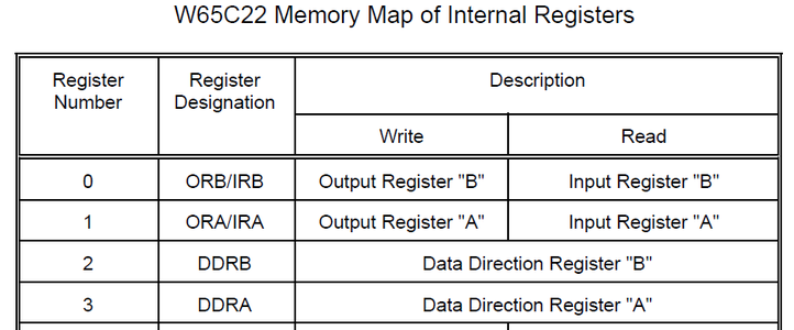
The 6522 has two I/O ports as well as many other features, but port A and B are easily accessible. To output data on the port, the Data Direction Register (DDR) needs to be set accordingly and the data sent to the port itself.
With the above set up, the 6522 is located at $E000.
To output data on port B, the DDR at $E002 is set to $FF (255 - all outputs) and data is sent to $E000.
To output data on port A, the DDR at $E003 is set to $FF (255 - all outputs) and data is sent to $E001.
The code below loads $FF into the 6502 A register and writes it to DDR B at $E002. It then loads $55 and writes it to ORB. The code is rotated (giving $AA) and written to ORB. The program jumps back tp $1005 and repeats endlessly. NOTE: the DDR only needs to be initialised once.
Address  Hexdump   Dissassembly
$1000    a9 ff     LDA #$ff
$1002    8d 02 e0  STA $e002
$1005    a9 55     LDA #$55
$1007    8d 00 e0  STA $e000
$100a    6a        ROR A
$100b    8d 00 e0  STA $e000
$100e    4c 05 10  JMP $1005
$55 in binary is 01010101 and $AA is 10101010 which causes the LEDs to alternate 4 on, 4 off.
Quick and dirty fix:
Replace the 74HC00 (Quad 2 input NAND Gate) with a 74HC08 (Quad 2 input AND Gate) and the 6522 is now located at $6000 instead of $E000. This moves it from the upper 32K to the lower 32K of the 6502's addressable memory.
Step 3: The Arduino Program and Output

As the 6502 has no RAM to read from, the Arduino is supplying the program for it to read. When a clock pulse is detected on pin 18, the Arduino puts the program data on to the data bus (Arduino pins 39,41,43,45,47,49,51 and 53). The 6502 generates its own addresses which are only monitored by the Arduino on the even numbered pins 22 to 52. The Arduino is also supplying the clock pulse on pin 37. The R/W line of the 6502 is monitored on pin 31.
As the Arduino is supplying the data, so far it has not been possible to get the 6502 to input data from the VIA (unless you know better).
The Arduino program is below and a sample output from the Serial Monitor is above.
Attachments

Step 4: Conclusion
Again I have tried to show how to set up a minimal "6502 Computer".
At this stage the 6502 is still relying on the Arduino to supply it with a program and a clock pulse in order for it to run.
It is a step further than when I set it up on bread board.
I have not used the 74HC373 this time but the more complex 6522 to latch the data outputs. Also the 6522 has two I/O ports.
I intend taking this project further by installing some SRAM or an EEPROM.