Introduction: Building JFET Preamplifiers for Musical Instrument Use.


By making a JFET amplifier, students will understand how JFET amplifiers can be constructed using different methods such as diode bias, resistive bias and the load line technique.
Since I first started properly doing electronics, I always liked the idea of an electronic component as essentially simple as the JFET.
The JFET was first theorized in 1925 by Julius Lillenfield but wasn’t built until much later. As much as the JFET was theorized many years before many bipolar junction transistors that you see today, it wasn’t built until much later. In amateur, they don’t have a very large amount of uses (unlike MOSFET’s and BJT’s).
If you observe the transfer curves of a JFET before saturation, it is very much like a triode’s transfer curve. This is a very linear region and will provide clean and uncoloured amplification. I have included a comparison picture of the common 12ax7 triode compared to a 2n5457 JFET. Another advantage of a JFET is that the gate has a very high input impedance, which is very useful to instruments like guitar in preserving the high frequencies. The downside to JFET’s is that they can at times have too low of a drain current to drive low impedance sources. Luckily, in this day and age, guitar amplifiers and post guitar effects generally have quite a high input impedance, for example, the humble Ibanez Tubescreamer features an input impedance of around 500k.
In JFET Based amplifiers, the input impedance is pretty much determined by the gate resistor which comes after the input capacitor to ground.
Step 1: Choosing the Design Parameters
In an ideal world, we could design a product where we set the design parameters and just choose the perfect product to fulfil this role. Unfortunately, there is not a very wide choice from JFET’s as not very many companies actually produce these. The general ones for sale (after a quick eBay search!) are: MPF102, J310, 2N3819, 2N5484 and 2N5457 (my choice of JFET). I will show the design step by step on how to design a JFET amplifier using any existing N channel JFET through looking at the data sheet of the product.
The parameters we need to design ourselves a JFET amplifier are:
• Vcc (Positive supply voltage)
• Minimum Rds On of the JFET (resistance of the JFET when fully on biased)
• Ids (Current flowing through the JFET from drain to source)
• Cut off frequency of the JFET preamplifier
• Vgs Cut off voltage
From these parameters, we can calculate the values for Cin (Input capacitor), Rg (Gate resistor), Rs (Source resistor), Rd (Drain resistor) and Cout (Output capacitor).
When designing the circuit, you must ensure you don’t exceed the voltage and current rating of the JFET. With the JFET I am using (2N5457), the maximum VDS (maximum voltage across the drain and source) is 25v, the Vgs (off) is -2.5v and the maximum Ids (maximum current across the drain and source) is 3mA. On the data sheet, the Ids is called Idss. All that Idss means is the current flowing through the drain of the JFET with the gate grounded. This value should not be exceeded and as a general rule, you should not exceed about 60% of the absolute maximum rating, this will prevent any broken devices and failures.
Since the majority of guitar circuits run off 9v, I will choose 9v as my Vcc. After comparing this to my data sheet value, my JFET will still be within the voltage range. For the current, unless you purposely need a low current circuit for battery saving or what not, I will just run my JFET at 60% of the maximum Ids. In this case, this is:
0.6 x 0.005A = 0.003, 3mA.
So far, we have chosen the vital parameters for designing a JFET amplifier.
Step 2: Choosing Values for Rd and Rs
This is where it starts to get a bit mathematical!
Now that we have the vital parameters (Vcc=9v, Ids=3mA Vgs(off)=-2.5v ) we can choose the value of the resistors Rs and Rd. In the data sheet for my Jfet, it didn’t say Rds (on) of the Jfet. Since this is always going to be in linear mode and not saturated, this is not a major worry and if you just put 0 into the equation, it cancels out the requirement for the Rds. Obviously, if Rds is specified on your datasheet, you can add this into the equation.
The first parameter we need to calculate is the total resistance of Rs and Rd. This requires the Vcc, Ids, Rds(on) and Vgs(Cut off).
So:
Rs + Rd = ( Vcc – ( Rds(on) x Ids )) / Ids
In my situation, this turns out as:
Rs + Rd = ( 9 – ( 0 x 0.003 )) / 0.003 = 3000 Ohm
So now we have calculated the total resistance of Rs and Rd, we must now calculate what each one will be.
Firstly, we must calculate the source resistor:
Rs = Rs + Rd x ( -Vgs(off) / 10 )
Once again, in my case, this will be:
Rs = 3000 x ( -2.5 / 10 ) = 750 Ohm
Calculating Rd from this is a the very easy task of:
(Total resistance of Rs and Rd) – Rs = Rd
Which in my case:
3000 Ohm – 750 Ohm = 2250 Ohm
From this simple maths and use of Ohms Law, we have calculated the vital parameters required for a JFET amplifier.
Since these values are not standard resistor values, we can just go for the closest values to them using the E24 series: http://www.logwell.com/tech/components/resistor_values.html
My resistor values will now be:
2250 is now 2.2k Ohm
750 is actually already an E24 series resistor value!
Step 3: Choosing the Values for the Input Filter and Output Filter.
Now that we have calculated the vital parameters of the Jfet amplifier, we can now calculate the cut off frequencies of the input and output filters. A capacitor with a resistor in this configuration produces a high pass filter. This can be calculated to work with another equation.
The equation for an RC filter (Resistor – capacitor filter) is:
1
---------------- = Frequency cut off at -3dB
2 x Pi x R x C
Now that equation may look daunting to some but its actually quite simple! It can be easily rearranged to find out the value of any product.
When designing this product for instrument use, we will want to make sure that the -3dB cut off point is BELOW the lowest frequency produced on the instrument to allow the signal to pass through cleanly. On a standard tuned guitar, the lowest frequency produced is the open E string at 82.4Hz.
We also want to ensure that the impedance of the circuit is high, to not load preceding effects or the guitar pickup. A good value of high impedance will be between 100k and 1Meg. If a higher value is used, the circuit will be noisier due to thermal noise of the resistor being amplified, along with noise within the JFET itself. I personally would use a value of 100k as my guitar has active pickups. The input impedance is set by Rg (The gate resistor to the JFET) since the JFET takes near to no current at the gate..
Now we know what the input impedance needs to be 100k and the cut off frequency needs to be <=82.4Hz, we can rearrange the equation to calculate C
1
---------------- = C in Farads
2 x Pi x R x F
One problem we have with choosing C like this is that capacitors don’t really come in a wide range of values, the values available to the average amateur electronic engineer is: 10nF, 22nF, 47nF, 100nF, 220nF, 470nF, 1uF, 2.2uF and so on.
If you put the values into the equation, you can calculate a value near to C that you will want to use. Once you have calculated this value, go for the capacitor value that is higher than this, e.g. if you calculate 159nF, go for 220nF.
So in our current situation, R = 100k and F = 82.4Hz
1
------------------------- = 0.0000000191F, 0.0191uF or 19.1nF
2 x Pi x 100k x 82.4
If we choose a value of 22nF, we will get a cut off frequency of 72.3Hz, this is below our lowest produced note by a standard tuned guitar. If you want the amplifier to have a full frequency range, you can make this capacitor a large value such as 470nF. This will produce a cut off frequency of 3.39Hz! This is sub sonic and below the human hearing!
The same applies for the output filter apart from instead of Rg, we now have Rl. Since we don’t actually know what the input impedance of the next product in the chain will be, we will just make Rl a nice standard and quite low value, such as 10k. Always make sure that Rl is larger than Rd. A standard value for the output capacitor is 1uF. This gives a cut off frequency of 15.9Hz. Low enough for nearly every instrument!
Step 4: Designing a JFET Amplifier Using the Load Line Technique


In this section, I’m going to tell you how to design a JFET amplifier using the load line technique. This was used many years ago to design original valve equipment and the same techniques can be applied to JFETs provided you have access to the drain characteristics chart.
How this works is you must be able to edit the chart in some way (for example using Microsoft paint or printing off the chart and doing it with a pencil.) and you must draw on the load line of your chosen values.
Since my chart only shows up to 1.2mA of drain current, I’m going to use a current value of 0.8mA at 9v so I can utilize my chart.
So the first step in using the load line technique is to believe it or not, draw a load line! A load line is literally a line that is drawn from the Vcc (drain to source voltage on this chart) to how much current will be flowing, so in my case from 9v to 0.8mA. This line will be used to calculate the bias point and the resistor value used for Rd and consequently Rs.
Calculating Rd is very easy in this case, it literally consists of:
Rd = 9/0.0008 = 11250 Ohm
To calculate Rs, we must now look at the load line and decide where we want our bias point. To bias the amplifier so it can have a full swing, we must choose the bias point in the middle of the load line. As you can see in my picture, I have put a little blue dot where the bias point lies. If you look at the chart, you can see the thick black lines, they are the characteristics of the JFET. If you see to the right of the chart, there are voltages (VGS values). As you can also see, my bias point lies just below the -0.4v point (between -0.4v and -0.6v) it is about -0.44v. All that this means is that if the gate is 0.44v LOWER than the source, it will follow this curve. Since we are pulling the gate to ground, we can achieve the same thing by putting the source to +0.44v. Therefore the gate is -0.44v relative to the source.
We can now calculate Rs:
Rs = V(Bias) / Id = 0.44 / 0.0008 = 550 Ohm
Now, the only problem with this method is if you look at the curves of the JFET, once you get past the linear region and into the saturation region, not much happens in terms of transconductance, you increase Vds and the Id hardly increases. This has a profound effect on the output waveform by squashing one end of the waveform. This can be very musical on guitar and adds a fair amount of second harmonic content (something lots of guitarists crave!). This can be changed by moving the bias point much more towards or away form the linear region, all of which can be done by replacing the source resistor for a potentiometer or variable resistor.
Once again, since these aren't standard value resistors, the values:
Rd = 10k Ohm
Rs = 560 Ohm
Could be used.
Step 5: Designing JFET Amplifier Using a Constant Voltage Source... on the Source!


The final method I am going to show you about JFET amplifier design is using a constant voltage on the source. This will maximise the gain but will not produce a perfectly symmetrical waveform depending on what JFET you use.
How this works is that the source resistor is being replaced for a diode. Different kinds of diode will work better with different JFETs. For example, a standard 1N4001 or 1N4148 diode will have a Vf (forward voltage drop) of about 0.6v-0.8v. Another type of diode is a BAT54 schottky diode which has a Vf as low as 0.3v. Each of these different types of diode will bias the JFET differently depending on the JFETs Vgs(on).
In the case of the 2N5457 JFET, using a 1N4148 biases the JFET colder than the resistor method (Cold biasing means the JFET is being starved of current and therefore, the voltage at the drain is going to be higher than Vcc/2. If I use the BAT54 diode, this still forces the JFET to bias cold, though less so than the 1N4148. With an LED, the circuit failed to work entirely.
How it works: This circuit works because a diode only starts to conduct until the Vf is exceeded. Therefore, if one is put between the source and ground, it will only conduct once its Vf is exceeded, that being around 0.6v so the gate is now at 0.6v with respect to the source, biasing the jfet. With the diode, the Vf hardly changes with the increasing and decreasing current, essentially keeping the source voltage constant.
I have included a picture of the Vf chart. The Vf increases by about 100mV at a change of 150mA which is going to be minute at the current used by the JFET.
Step 6: Now You Have Finally Designed Your JFET Amplifier! (Hopefully!)

Now hopefully, you have designed yourself a JFET low power amplifier! Hopefully yours is working but if not, look through the connections on the JFET, they generally do not match standard transistor pinouts. If that isn’t the problem, check at the drain of the JFET and make sure that the voltage is <9v. Also check for a small voltage at the source of the JFET (Should be between 0.5v and 2v dependant on your JFET).
On the next few pages, I will tell you some improvements you can make.
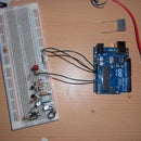
Step 7: Building the JFET Amplifier on Breadboard


Building a JFET amplifier on a breadboard is also an incredibly easy task as it generally required no more than 7-8 components! The parts list of the amplifier I built is:
• 2N5457 JFET
• 1x 10k Resistor
• 1x 2.2k Resistor
• 1x 820 Ohm Resistor (I didn’t have a 750 Ohm resistor)
• 1x 100k Resistor
• 1x 22nF Capacitor
• 1x 1uF Capacitor
For my input capacitor, I used a Poly cap and for the output I used a Philips electrolytic cap. Many people are against the use of electrolytic caps in the audio path but I think these Philips ones should be an exception because they are of exceptional quality ;).
Step 1:
Assemble the components you are going to use and make sure they are of correct value and suited to the job.
Step 2:
Place the JFET in the breadboard and ensure to note which leg is what (this can be found on the data sheet, I will include a picture of my 2N5457’s legs in the pictures).
Step 3:
Add resistors in, in my case, my JFET was in rows 56, 57 and 58 (56 being the gate, 57 is the source and 58, the drain.) my 2.2k resistor goes from row 58 (the drain) to the positive supply (this resistor is Rd), my 820 Ohm resistor goes from row 57 to ground (this resistor is Rs) and finally, my 100k resistor goes to ground too from row 56 (this is the Rgate).
Step 4:
Add the capacitors in, the 22nF capacitor goes from row 56 to the input (this is the input capacitor!) and the 1uF capacitor goes from row 58 to the output (this is the output capacitor!). If you have added the gain mod, the 10uF capacitor goes from row 57 to ground.
Hopefully you should have now built the amplifier successfully! Well done.
Step 8: Adding More Gain (Or Treble Boost)!
If you don’t feel that your JFET amplifier is providing you with enough gain, you could firstly cascade multiple stages to produce the gain required but this can be much pricier than a simple trick I’m about to tell you.
It is possible with just the addition of a capacitor to increase the gain of the amplifier by a quite large margin! This amount of gain added is not going to be a fully calculated value as it will vary with frequency but should generally increase the gain by 2-3 times.
This is achieved by putting a capacitor in parallel with the source resistor. How this works is it gives a low resistance path for the AC to flow. A Capacitor has something called reactance with AC signals which is equivalent to AC resistance and decreases as current increases. By putting a large-ish value capacitor across the source resistor of the JFET, we can provide this low resistance path for AC while keeping the DC bias of the JFET correct.
This capacitor value is calculated the same way the filters are calculated with R being the value of Rs and F being the minimum cut off frequency again.
One way this can be utilized though is in creating a treble boost circuit. If the cut off frequency is set quite high, say 1kHz, the frequency response will be flat until a bit before 1kHz where it will start to rise and boost the treble section of the waveform. A suitable capacitor value for treble boost with my source resistance would be about 0.22uF
I simulated this circuit in LTSpice to produce a plot of frequency vs gain to show what the treble boost frequency response looks like.
Step 9: The End.
Well done! You should now know the multiple ways to build and bias a JFET amplifier stage. Any questions, go ahead and ask, I’ll be more than happy to answer! :)
I have also included a couple of tracks recorded with this circuit:
• ESI Maya44 USB Soundcard
• Yamaha Pacifica S-S-H guitar
• HP DV6 Phenom Quad core
• Audacity with Gverb Plugin
I added a touch of reverb to each one just to give a roomy feel since I recorded DI. Btw, excuse my terrible playing! I’m really not in the slightest bit a guitarist, I play bass as my main instrument, without a pick so when I have to play with a pick, I revert to a 2 week guitarist! :P


Participated in the
Education Contest