Introduction: Implement Your Own Transistor Logic Gates


A lot of logic gate implementations are already on the web for reference and this instructable is just one of my attempts to implement my own. Do note that the circuit designs that I came up with in this mini experiment (experiment...YES! this is just one way to waste my time) are not recommended for any serious applications (although i will be using this for my future projects since i don't feel like buying an IC version of logic gates yet).
===============================================
For questions, concerns, clarifications, corrections etc
email me at: mttarvina@up.edu.ph
===============================================
Suppose we want to implement logic gates that strictly follow a certain criteria:
--> INPUT and OUTPUT HIGH is equal to Vcc (in this case, I used a constant 9V supply as Vcc)
--> INPUT and OUTPUT LOW is equal to 0V
This is just the ideal criteria that i want to impose in my implementation. In the actual circuit, an OUTPUT HIGH of 9V(Vcc) may or may not be attainable due to component limitations but i'll try to make it close
Given a logic gate with same implementation as defined above, i can cascade a lot of them to create a system of logic gates with certain application. Since i intend to cascade transistor logic gates, i have to minimize the loading effect of each gate/stage in order to maintain the criteria. After taking into account the loading effect, its time to think of the design.
Step 1: Functionally Complete Set

There are a lot of logic gates with unique response to logic inputs. For now lets focus on logic gates with one to two logic inputs namely: NOT, AND, OR, NAND, NOR, XOR, XNOR and many others. If we want to implement each one of them, it would take a lot of time to design a circuit. Implementing some of the gates might need a lot of transistors in the actual circuit. Well, i don't like that.
By this time, we have to realize that some logic gates can be formed by a combination of two or more logic gates. Taking this into account, i decided to design a circuit just for one or two logic gates that would form a functionally complete set. This set would span all the other logic gates and any logic gate can be implemented by a combination of the elements of the set.
Here are some of the examples of Functionally complete sets:
--> {AND, OR, NOT}
--> {AND, NOT}
--> {OR, NOT}
--> {NAND}
--> {NOR}
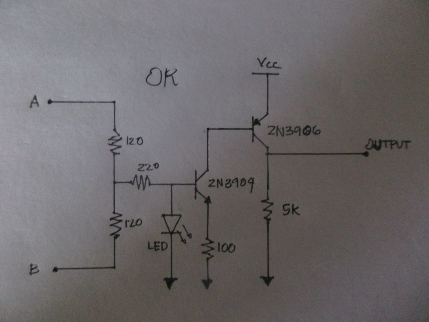
Choosing a design for a functionally complete set makes the work a lot easier since we can just cascade a combination of its elements to create the design for the others. In this case, i chose the set: {OR, NOT}
The OR(+) gate and the INVERTER (NOT ~) has the following characteristic as shown in the image (A and B are logical inputs).
Here is how to implement some of the other logic gates using the set {OR, NOT} :
*Implement a NAND gate:
~(AB) = ~A + ~B
*Implement AND gate:
AB = ~~(AB) = ~(~A + ~B)
*Implement NOR gate:
~(A + B)
Step 2: Circuit Design


In the design of both OR and NOT gate, I used a PNP transistor at the output. Based on experience, a PNP transistor has a lower Vce(sat) or a minimum collector-emitter saturation voltage when operated at , guess what, .. the saturated region. Sometimes it reaches 0.5V or even as low as 0.05 mV when you greatly increase the Vbe of the transistor just below its maximum value before IT BLOWS UP. But why do we want a much smaller Vce(sat) ? So that the output would be pretty close to Vcc following the said criteria earlier.
In the circuit schematic, the Vbe of the output PNP transistors are measured to be more than 0.73V enough to operate it at the saturated region. You can however modify the design to push it further and have a Vbe of more than 1V. Just be careful not to supply it with more than 6V since if i'm not mistaken, 6V is the maximum Vbe allowed to operate the transistor (check datasheet).
Also because of the PNP configuration at the output, when the transistor is in cut-off region, the OUTPUT goes as low as 0V because of the 5K resistor connected to ground again, following the said criteria.
Now how about the loading effect? Well, because of the transistor configuration at the output, loading effect would be negligible and regardless of the output load, the output voltage would still be constant since it doesn't change the fact that we are forcing the output transistor to operate at saturation/cut-off and it is mainly dependent on the value of its Vbe, not the output resistance. In this way we can cascade any combination of the two logic gates without any compensation on the input and output terminals of each stage/gate.
Step 3: Building the Actual Circuit


We have the following needed materials:
-Constant DC power supply (9V output)
-2pcs 2N3906 PNP transistor
-1pc 2N3904 NPN transistor
-2pcs 5K ohm resistor
-2pcs 20K ohm resistor
-2pcs 120 ohm resistor
-1pc 220 ohm resistor
-LED (2V forward voltage)
Construct the circuit as shown in the circuit diagrams. Use jumper wires if necessary.
Step 4: Testing the Circuit

The measured data is listed as follows (shown in the image) for each logic gate implementation.
Note that connecting the input to ground would result to the same output as when letting it float (although you would have stray noise voltage signals up to hundreds of millivolts at the input pin)
Based on the tabulated results of this mini experiment, I can safely conlude that I can definitely cascade these two logic gates to implement the others while still maintaining the said criteria earlier. One can also use different levels of input voltages that would result to an INPUT HIGH or an INPUT LOW or even force the output transistor to operate at a forward active region. However, the OUTPUT HIGH would always be close to Vcc (when output transistor operates at saturation) so its better to use an input voltage equal to Vcc or in this case, 9V to be consistent especially when cascading gates.