Introduction: PCB Design Tutorial - How To Design Your Own PCB Board


When you are going to design your own PCB, you need to draw holes, pads and wires for your circuit. Then you send this drawing to a manufacturer or you etch it yourself.
Starting with schematics
Before you start drawing wires and stuff, you need to know what circuit you want to build. So you need to find or design schematics for your circuit. And you need a PCB design software. Then you are ready to begin the process. Start by drawing your schematic diagram into the software you have chosen. Here we’ll use the free PCB design tool EasyEDA to show how to design a circuit board with Example PCB of Voice Modulator Circuit.
Voice Modulator Circuit
We are going to make a Voice Modulator Circuit, by using self-designed PCB. This is a fun project, mainly designed for changing or altering the voice. Generally, when we speak in a MIC we hear same voice. But in this project when we speak in MIC, we will hear a little bit different voice something like a robot is speaking.
Circuit Diagram and Description:
This Voice Modulator Circuit is made by using LM358 op-amp and LM386 Audio Amplifier IC. User can use 3 volts to 9 volts to drive this circuit. In this circuit we have changed voice by using band-pass filter circuit which is made by using op-amp IC and a R10 pot is used for change the gain of the MIC preamp circuit. IC LM386 is used for amplifying the voice modulator signal. At the output, we have two choices for listening the modulated voice: speaker and 3.5 mm jack for headphone. Pot R5 is used for volume control. Jumper J2 is used for the gain of the audio amplifier.
You can access whole Circuit and PCB layout for this Voice Modulator Circuit by following the below link:
https://easyeda.com/circuitdigest/Voice_Modulator_Circuit-e59a40c5a2df413b83fc4d5c886f5140
Step 1: Steps to Design Circuit and PCB Board Using EasyEDA:

In first step user need to open EasyEDA website and then sign up if using for the first time, otherwise sign in with your credentials.
Step 2:

New project " https://easyeda.com/editor " and open schematic by clicking over New Schematic (blue circle) or the user can directly make the PCB layout by clicking over new PCB (red circle) as shown in below picture.
Step 3:


Now you will see the schematic window where user can select the required components from the EasyEDA library from the left hand side panel of the website. User can see the symbols of the resistor, capacitor, inductor, power etc. and can place any item over the schematic by clicking over it and then move the cursor to the place where you want put that component and finally click again to place it.
If you want to get more components then he/she can go with more libraries search option on the left down side of the screen.
Then will get another window for selecting components with category and search option. And that is how user can get the desired component.
Step 4:


After getting all the components, next part is to connect components to each other and to do this EasyEDA has a Wiring Tool window. In this tool, by selecting wire we can connect the components by clicking on start point and then click on end point.
As you can see we have started to draw the Voice Modulator Circuit as shown in above figure.
And here we have completed the Drawing and its time to write the text over the schematic by choosing " T "option from the drawing tool. Here we have shown that in the red circle in the given picture.
Step 5:

Now you need to connect Vcc and Ground to the circuit. To do so, you can select power and Ground from the EasyEDA libraries in left-hand side of the screen.
Step 6:

Finally you can save the schematic by selecting the blue folder icon as shown below and click on Save, then save it by giving proper Name to the schematic.
Step 7:


Now the circuit is ready for PCB layout conversion. For PCB layout user needs to move the cursor over fabrication tab as shown in below figure. Here you will see convert Project to PCB and by clicking on it,you will redirect to PCB layout window.
Step 8:

Now you need to place all the component over the desired place and also save the layout as we saved the Schematics.
Step 9:


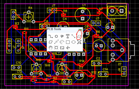
You can route the circuit manually with the help of PCB tools or there is a Auto routing feature in EasyEDA (red circled), which will automatically route all the connections for you.
Here in given picture below, user can set Track width, clearance (trace clearance), layer and other things before Auto routing and then click Run.
Then you will see that auto-routing will starts, and after few seconds it will complete.
Step 10:


And then you will see the given result. Now you may place copper pour over the top side and bottom side as well by selecting copper pour in PCB tools
Top Copper Pour by selecting top layer (see black circle in below picture), then bottom layer.
Finally we have our PCB layout Ready.
Step 11: Getting Your PCB Manufactured

When finished drawing the board, it is time to get your PCB design ready for manufacturing.
This basically means you need to check your board for errors and convert your board layout to Gerber files. Then, choose a cheap PCB manufacturer and get your board made. We have used EasyEDA PCB manufacturing service to manufacture the example PCB.
Step 12: Calculating and Ordering PCB Samples Online:


After completing the design of PCB, you can click the icon of Fabrication output above, it will take you the PCB order page where you can download or view gerber files of your PCB and send them to any manufacturer, it’s also a lot easier (and cheaper) to order it directly in EasyEDA.
You can directly order this PCB or download the Gerber file using this link.
Step 13:


I ordered 5 of the Voice Modulator PCBs from EasyEDA, and they arrived at my door two weeks later. After an inspection, I could see that the PCBs were well made, and no defects could be found on any of the boards. Electrically, the PCBs work perfectly. If you want, you can clone my Voice Modulator Schematic and PCB here and start to design your own PCB board.

![Tim's Mechanical Spider Leg [LU9685-20CU]](https://content.instructables.com/FFB/5R4I/LVKZ6G6R/FFB5R4ILVKZ6G6R.png?auto=webp&crop=1.2%3A1&frame=1&width=306)