Introduction: Preparing a Schematic


Before we can lay out our circuit board we need to do a host of preparatory work. This includes creating a schematic both on paper and digitally, and setting up a project within the Eagle software. Creating a schematic is not just a helpful step, but a necessary step in the Eagle design process. The circuit board file is linked to the schematic file, and any change you make to the schematic will eventually have an effect upon the layout of the board. Albeit this may all seem like a lot of extra work, you will be glad you did all of this later.
Step 1: Draw a Schematic

I'm going on the working assumption that if you want to make a PCB you already know what a schematic is and how to draw one. If you don't, I highly recommend first completing my basic Electronics Class.

To begin, draw out a schematic of your circuit on a piece of paper, using the breadboard as your guide. Even if your circuit is copied from a different one, draw it out again. Perhaps you changed a connection or a value of a component and forgot about it, or perhaps the original circuit was drawn incorrectly. Either way, you want to make sure you have drawn the definitive schematic of the circuit you are making, drawn in a manner that quickly makes sense to you. This schematic will later serve as your blueprint for making connections in the design software.

It is helpful to use a pencil in case you draw something incorrectly and need to quickly make a change. For instance, I forgot to add in a DPDT switch that lives off of the breadboard and is used to toggle the audio signal routing.

When I'm done and sure the schematic is correct, I like to trace the whole thing in marker to finalize it. Pencil tends to fade or get rubbed away over time.
Once it is traced, I then like to erase the remaining pencil marks to make it nice and pretty-looking.
Step 2: B.O.M.
B.O.M. stands for Bill of Materials. This is the entire list of materials for your circuit. This can easily be created by making a list of the components you see in the schematic.
To make matters even easier, I numbered each component in the schematic (the "Name" field below). This makes sure I don't leave any of the parts out as each part should have a unique value in the materials list.
For my schematic, the B.O.M. is as follows:
| Quantity | Value | Name | Supplier | Part Number |
| 2 | 10K | R1, R2 | Digikey | CF14JT10K0CT-ND |
| 1 | 100K | R3 | Digikey | CF14JT100KCT-ND |
| 1 | 4.7K | R4 | Digikey | CF14JT4K70CT-ND |
| 1 | 47K | R5 | Digikey | CF14JT47K0CT-ND |
| 1 | 1M Potentiometer | R6 | Mouser | P160KN2-0EC15B1MEG |
| 1 | 1K | R7 | Digikey | CF14JT1K00CT-ND |
| 1 | 100K Potentiometer | R8 | Mouser | P160KN-0QC15B100K |
| 1 | 100uF | C1 | Digikey | 493-13464-1-ND |
| 1 | 0.01uF | C2 | Digikey | 399-9858-1-ND |
| 1 | 0.1uF | C3 | Digikey | BC2665CT-ND |
| 2 | 22uF | C4, C5 | Digikey | 493-12572-1-ND |
| 2 | 1N4001 | D1, D2 | Digikey | 1N4001-TPMSCT-ND |
| 2 | 1N34A | D3, D4 | Digikey | 1N34A BK-ND |
| 1 | 42TL013 | T1 | Mouser | 42TL013-RC |
| 1 | TL071 | IC1 | Digikey | 296-7188-5-ND |
| 1 | DPDT pushbutton | SW1 | Mouser | SF12020F-0202-20R-L-051 |
| 1 | 1/4 stereo | J1 | Mouser | 502-12B |
| 1 | 1/4 mono | J2 | Mouser | 502-12A |
| 1 | 9V battery | B1 | Digikey | 36-232-ND |
Step 3: Setup Eagle CAD
Once we have our schematic and BOM sorted out, the next order of business is to setup Eagle CAD.
Launch the software. First it will ask you to login using your Autodesk ID and then it will launch the Control Panel.

Expand the Projects folder list on the left-hand menu, and then select the Eagle folder.
Next, either select (File > New > Project) from the top drop-down menu or right-click on the folder and select "new project" to create a new Eagle project. Name the project after the circuit you are making, and hit enter on the keyboard.
Our digital schematic and PCB design will live within this project. However, before we can access those, we need to create them.

To begin we will create just the schematic. The board file will be created later, once we have the schematic nailed down.
To create the schematic, select the project you have just created and then select (File > New > Schematic) from the top drown-down menu. Alternately, you can right-click on the project and select the same. A new schematic window should load.
Save this window by selecting (File > Save) or pressing command+S to load the save menu. Name the schematic whatever you want (like "Flying Monkey Zebra"), but I find it helpful to call is something intuitive like "[name of project] schematic"
Step 4: The Eagle Interface

Eagle is a complex software package intended for creating complex circuit boards for mass production. By contrast, we will be using it to create a rather simple circuit board for personal use. Thus, when you look at the interface you will notice there are a lot more options and buttons than we will actually be using in our first design.
You may not easily understand (and may never fully understand) the Eagle interface and, to be truthful, is not always intuitive to use. However, patience is key. Don't lose heart or become intimidated by the interface. Once you get the hang of it, creating a simple board is — well — simple. You can always learn additional features later as your skill progresses. The core features that we will be using will be introduced throughout this class as needed, and don't require any sort of advanced degree.
Step 5: Creating a Digital Schematic

Before we can create a board, we want to recreate our schematic within Eagle. This will allow us to easily convert it into a PCB and helps to make sure all of the parts and connections are made correctly. This may seem like extra work, but will make life dramatically easier in the long-run.

In theory, you could have skipped the paper step and gone straight to this step, but I find having a paper copy is useful for two reasons. First off, having a definitive hard copy is nice simply for record-keeping. I recently rediscovered a circuit board I made for a custom guitar pedal almost 10 years ago, and had no clue what the circuit was or what value components I needed. The digital files were lost to time, and even if they weren't, the file formats I used at the time are surely obsolete. However, I am still able to quickly and easily find the paper schematic and B.O.M. in my project archive. Now would also be a good time to start a project archive if you don't have one.
The other reason I like to first make paper copies is that they will include all of the components even if they are not attached directly to the circuit board (in my case, the DPDT switch). On occasion, the digital version might omit it, as parts not directly attached to the PCB are not always necessary to include in the schematic (this will make more sense in a little bit).

If you look at your schematic window, you will notice it is blank. This is because we have not placed anything there yet. Let's fix this.
To begin, click the button on the left-hand side that looks like a plug with a Swiss flag over it, and says "add" when you mouse over it. This will load a window of all of the stock Eagle components.
In the search box type in "Frame." This should load a list of possible decorative frames for your schematic. I recommend selecting an A3-sized (standard printer paper) frame, but pick whichever you think will work best for your schematic and select "OK."
Click anywhere within the blank window to place the work frame. Then, exit out of 'add component' mode by hitting the escape key (esc) twice on your keyboard.

You have just placed a work frame for your schematic. You can view it by selecting the magnifying glass with a thick rectangle within in it on the top of the schematic window. This will "zoom to fit" to your work area.
As you may have guessed, adding a frame is not entirely necessary, but it helps keep things organized and pretty. Also, the versioning information on the bottom right-hand corner of the frame should auto-update as you save your work, which is a nice touch.
To observe this in action, save your schematic by selecting (File > Save) from the top menu or pressing command+S. I recommend saving your work often throughout this process.
Step 6: Add Symbols

Now is time to add all of the rest of your component's symbols to the schematic. Grab your B.O.M. and let's get to work.
Just like you did with the frame, select the "add part" tool, find your parts, and then place them into your schematic.

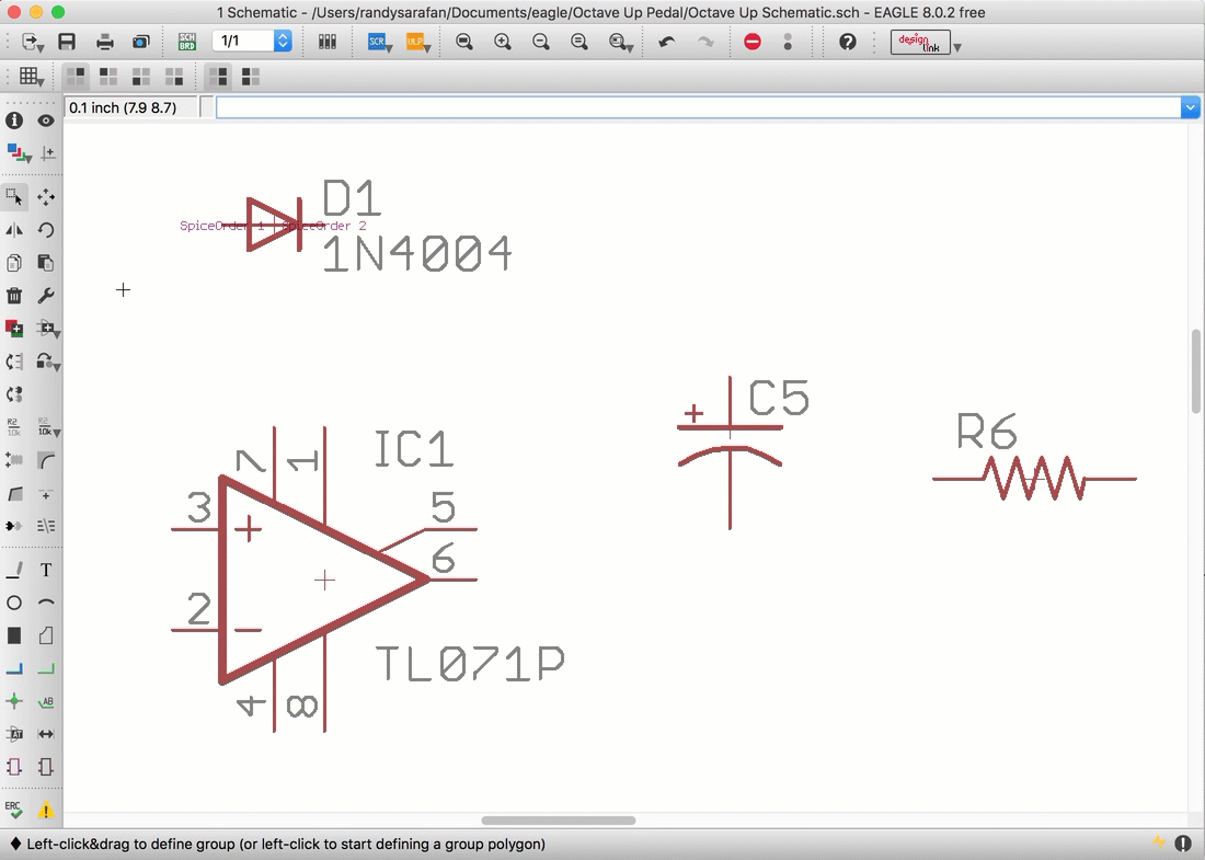
To begin, let's try something easy. Let's search for "op amp" and find the TL071 op amp that we are using in the schematic.
Notice that the part has a drop down arrow. What this means is that the part has multiple packages (surface mount and through-hole) and also has different footprints to choose from. You need to select the footprint for the board you will be using. If you select the surface mount footprint for a through-hole part, you will not be able to assemble your board correctly.

You can tell the difference between a surface mount and through hole part because surface mount will have an abbreviation which starts with "S" and through-hole will have an abbreviation which starts with "D." Aside from the obvious naming conventions, surface mount parts will have pads without holes in the center because the pins are mounted to the surface, and through hole parts have pads with holes in the center because the pins are passed through. It's actually fairly intuitive.

If you look for a resistor, you may be overwhelmed by about a
billion different resistor options. Knowing which one to select can be tricky. It's simply a matter of finding the right footprint. Your part supplier should have it's package listed on the product page, which, in turn, should indicate the best footprint to select. Often it is also important to consider the listed measurements (in mm) of the component in relation to the package.
For instance, if we were to look up a 10K resistor we will find that it has an "axial" package. This lets us know it is through-hole, but it still does not tell us the exact footprint we need since axial resistors come in a wide range of sizes. Fortunately, they also let us know the dimensions are 2.3mm x 6mm. From this information we can determine that we need a resistor package with at least 7.5mm spacing between leads (since bending the leads for through-hole mounting requires some additional width). However, to be on the conservative side, I decided go with 10mm spacing between leads.
When the software states "grid 10mm" under the part attributes for this through-hole resistor footprint, it indicates that we have found a resistor package with a 10mm lead spacing and ultimately what we are looking for.

Alternately, this is also where calipers can come in handy. Instead of looking up the lead spacing, we can simply measure the lead spacing and use this measurement to figure out what part footprint to select.
Calipers can also be used to double-check that the measurements given online are correct if something seems fishy.

Sometimes you won't find exactly what you are looking for. In those instances, you can find a similar part with an identical footprint. For instance, I could not find a 1N34A germanium diode, but it has a DO-07 footprint. Instead I am going to use an AA112 germanium diode which also has a DO-07 footprint.
For our purposes, this should be good enough. It will show up on the board as a diode with the correct footprint, and for what we are currently doing, that is all that really matters. If you were going to get deep into Eagle and start running circuit simulations, this might make a difference. However, that is well beyond the scope of this class and our goals.

If you really cannot find anything close to resembling your part, hope is not yet lost. Some manufacturers and part distributors will provide an Eagle parts library for their inventory. A good place to start to look for those is the Element14 Eagle CAD library page. Alternately, you can try googling for a library as well. If that fails, you can always create a new custom part.
To add the library go to (Library > Use...) on the top menu bar. Navigate to and select the library you downloaded and click "open." It will appear nothing happened, but when you now go to add a new part, your new library will be included.

Finally, we need to figure out which components from the schematic don't get mounted directly to the circuit board. In my circuit these parts include the potentiometers, audio jacks, battery snap, and bypass switch. In fact, some of these parts get wired directly and may not have connections to the board at all.
What I need to figure out is precisely what input and output points the board needs. After some thought I concluded I need an audio input and audio output, a connection for the drive potentiometer, and a power connection. To create these terminals, I am going to use the single "pin headers" from the Adafruit library I just downloaded.
Note that there are other "pin headers" I could have used already included with the software, but I just wanted to demonstrate adding a component from the new library.
Step 7: Draw Connections

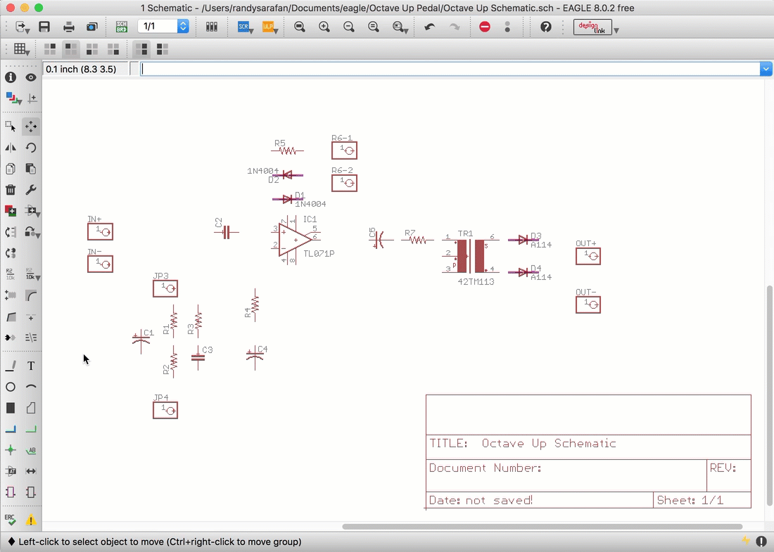
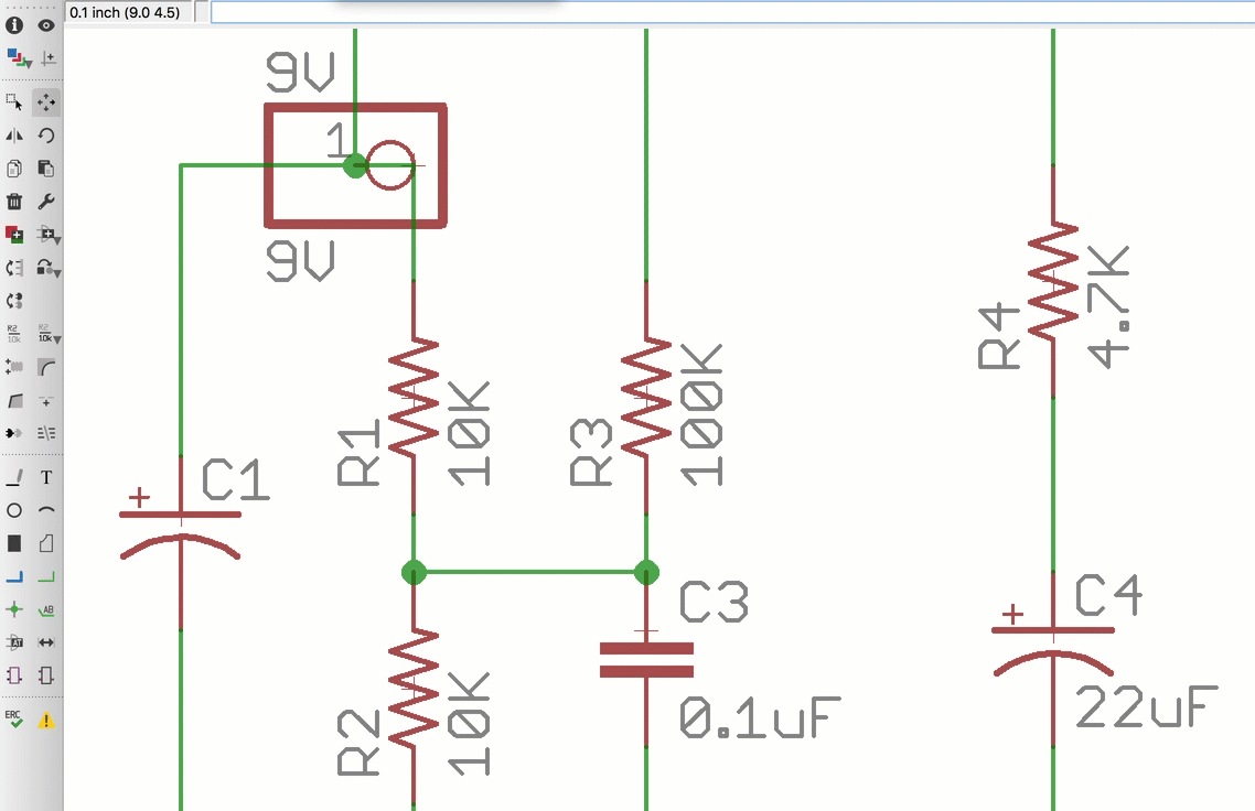
Once all the symbols are placed, we need to arrange them, name them, and draw the appropriate wire connections.
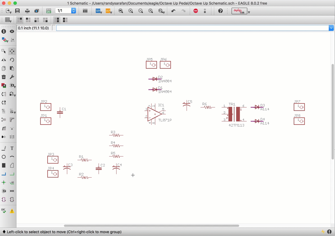
Select the move tool from the left-hand toolbar (it looks like a compass with four arrows), and click on the symbols to drag them into place. Arrange them on the screen to roughly match the layout of the hand-drawn schematic.
You may notice that sometimes when you click and drag on the symbol it does not go anywhere. This might be frustrating to you, and you might think the software is broken. It isn't that you are doing something wrong. You can only ever select and perform an action upon a symbol when the cross-hair from the tool overlaps the cross-hair on the symbol. Sometimes the cross-hair on the part might be hidden under a symbol or in a corner, making the whole endeavor kind of frustrating.

When appropriate, you can easily rotate the symbols by selecting the rotate tool and then simply clicking on the symbol you want to turn. With each click they will rotate 90 degrees.
The symbols should already have names, but these names may not correlate to the ones already assigned on our paper schematic and B.O.M. Thus, we want to use the Name tool on the left-hand toolbar to reassign the names of the components as appropriate. These names will transfer over to the PCB when we generate it, so it is important that we get them right.
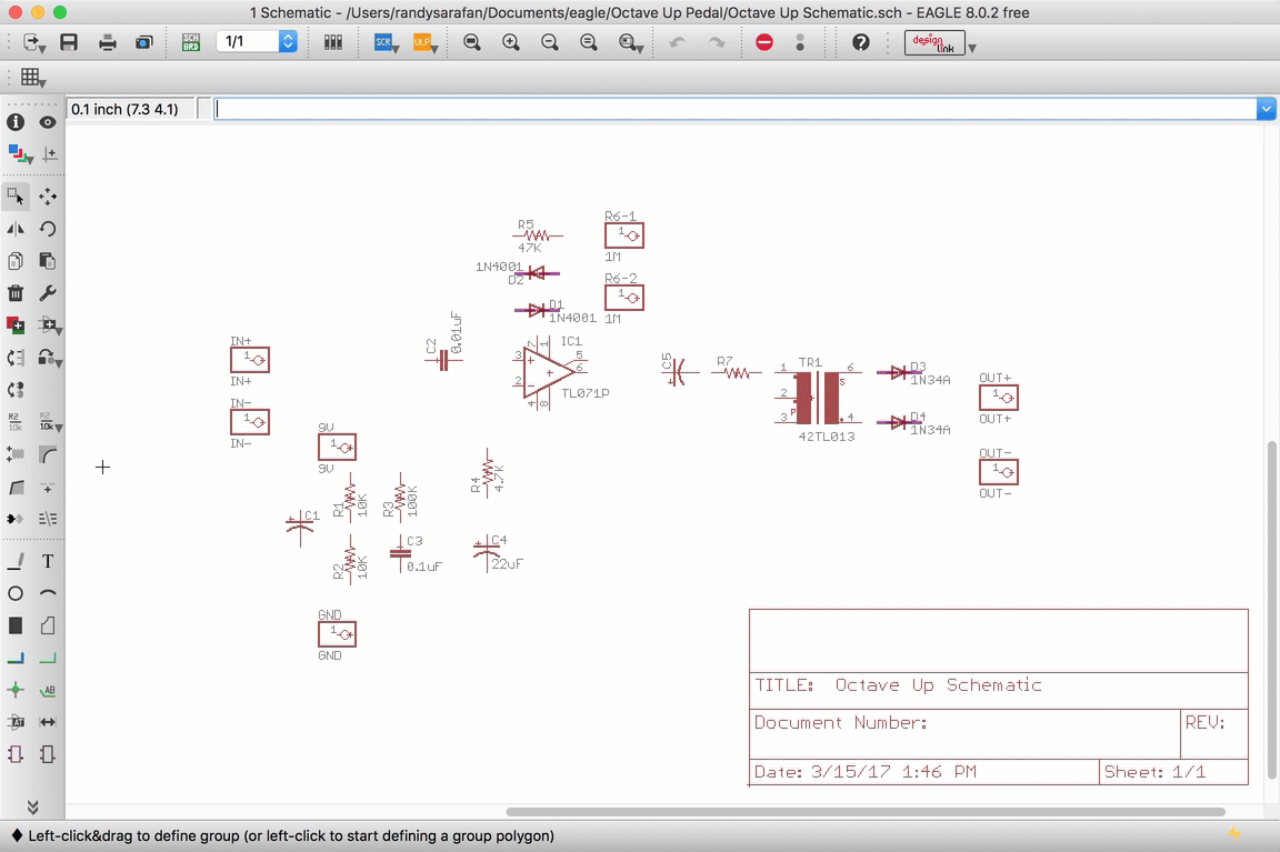
Next we are going to assign values to each symbol using the value tool from the left-hand toolbar. Whereas the symbols have names which specify what sort of part they are, the value designation lets us know what the part actually is. For instance, we can specify whether the resistor R2 is 100 ohm or 10K ohm (as is the case). It should go without saying why assigning values to the symbols is as equally as important as giving them each unique names.

Many of the schematic symbols look the same, even if they have dramatically different footprints. This is particularly true of the capacitors in my schematic. I am going to confirm that each schematic symbol correlates to the proper component by using the info tool from the left-hand toolbar to double check its footprint is correct.
In my case the footprint of the component matches my part perfectly, but if the footprint were not matched to the component, I would then check what other capacitor was incorrect and simply reassign the components that were mislabeled.

Once all of the symbols are arranged and labeled correctly, now it's time to connect them together. To do this we will use the NET tool to create connections between the symbols. All of the connections we make match our hand drawn schematic, with the exception of the components that we have determined do not mount directly to the board. In these cases, we just need to make sure the appropriate pin headers get connected to the appropriate spots.

Often connections will overlap one another without actually connecting. You can tell the difference between a connection and an overlap by the presence of a green dot. For instance, both diodes connect together with the output pin header because all three lines converge at the green dot. However, pins 1 and 2 do not connect together because there is no dot even though they intersect.
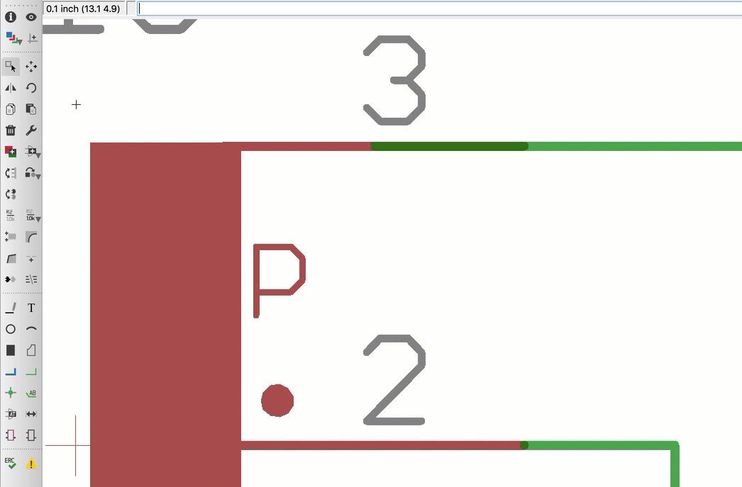
Sometimes you might make a connection which looks okay on first glance, but is not a connection at all. You can see an example of a bad connection here on pin 3. The long darker green overlapped section indicated that there isn't actually a connection there. An actual connection should look like the small green dot on pin 2.
To fix this, you need to delete the green line by selecting the Delete tool from the left-hand toolbar. This is easy to find because it looks like a little garbage can. Once the tool is selected, click on the line to delete it, and then you can go back and redraw the line with the NET tool.
When you have a lot of symbols connecting with one another, your circuit can get confusing very quickly. An easy way to tell if a connection is good is by moving the symbol you are unsure about and observing to see if the connections get dragged along with it. If they all appear to move around with the symbol, the connections are reliable.

Finally, once all of the connections are made and you have meticulously double-checked your work to make sure that it matches your hand drawn schematic, you are finally ready to make a circuit board.
Now would be a good time to get up, stretch your legs, eat a sandwich, or — if you are gluten free — have some rice pasta. If you are feeling particularly inspired, maybe even go for a walk. You need to reset your brain for the next lesson, and some exercise wouldn't kill you.

![Tim's Mechanical Spider Leg [LU9685-20CU]](https://content.instructables.com/FFB/5R4I/LVKZ6G6R/FFB5R4ILVKZ6G6R.png?auto=webp&crop=1.2%3A1&frame=1&width=306)