

Introduction: Build an 8-bit Microcontroller - Part II. - Program Counter


I am back with more!
Last time we started with transistors and fought ourselves all the way to gates, latches, flip-flops, and finally two of their many applications: 4-bit latch and 4-bit counter. These two are at the heart of our first AGR microcontroller PCB, the Program Counter module. Read through this instructable episode to discover how to create a 16-bit presettable counter from simple ICs available out there.
Supplies
To create along the instructable, you will need a couple of things:
- Patience
- Program Counter PCB, a breadboard, perforated board, or whatever the component carrier will be
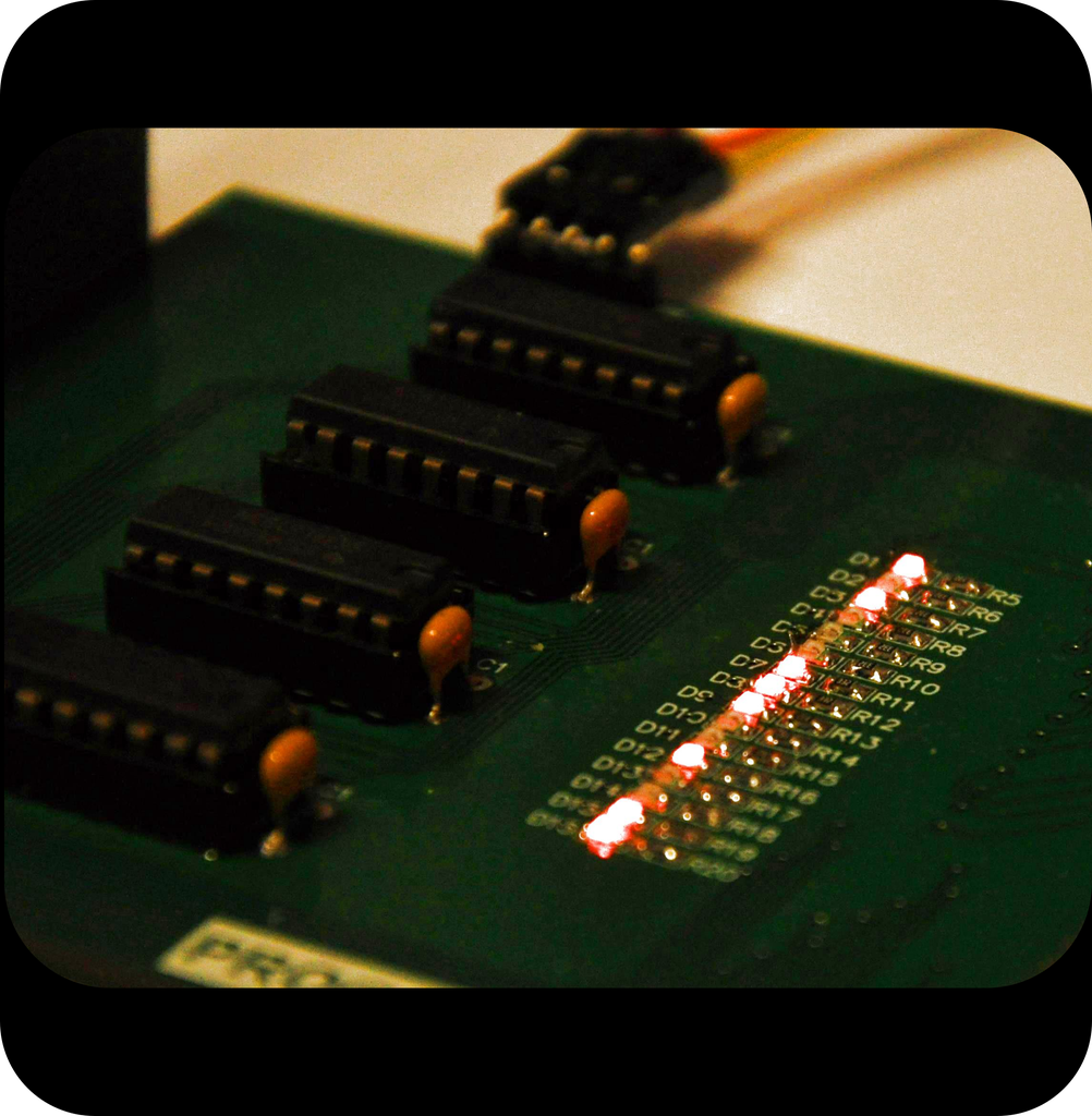
- SN74LS193N presettable 4-bit counters, four pieces
- Some LEDs for the outputs, along with the current limiting resistors
- Pin headers for the Address and Data buses
- Soldering and some other lab equipment, PC, benchtop PSU, 3D printer
- AGR Micro stimulus and flashing unit
Step 1: Continuing From Latches and Counters

If you guys still remember where we left off in the previous episode, it was two example applications for flip-flops, a 4-bit latch, and a 4-bit counter.
It is not by chance that I picked these two of all the possibilities out there: I picked them because this is something that is very much likely to be seen in all microcontroller architecture block diagrams in the shape of a program counter. We need to be able to cycle through memory addresses in order to fetch instructions from those addresses, and we need to be able to overwrite the content of this counter should there be a need to jump to a function call someplace else in the program memory.
Of course, a 4-bit presettable counter wouldn't get us very far since we would only have room for 16 instructions which isn't very much. I planned something bigger since I had some components lying around that I simply WANTED to use, especially after this 74LS193 fiasco. I don't want to get into this at the moment, but I managed to hit a couple of brick walls with the Program Memory module as well. More of this in the next episode!
Anyway, I decided to build a 16-bit Program Counter module that gives me 65536 instructions - more than enough for a proof-of-concept application like this microcontroller. The 74LS193N datasheet can't stop praising this thing as the best counter ever made, I think it's OK, and I like the fact that it's fully cascadable: the input of one stage can be connected to the output of the previous stage. I cascaded 4 such counters and wired the CARRY outputs further to the next stage's UP count input. The DOWN pin was tied directly to VCC (5V) while BORROW was left floating. This was done because there is no scenario with the Program Counter module where the PC should decrement.
Step 2: Libraries, Schematics and Layout


Design inputs:
- Increment needs to be supported? Yes
- Decrement needs to be supported? No
- Overwrites need to be supported? Yes, for jumps
- Bit count? 16
- Other ideas? Yes, LEDs on the address bus
- Must have a concept that allows the PCB to be inserted into a backplane of some sort
Even though I designed the Program Memory module first, I decided to present the Program Counter in the first episode detailing the modules - this way it is simpler for you dear readers ease into the project and have better continuity between the simplest element (transistor) and the end result (microcontroller).
As said before, I picked this part because I had it in stock. I drew the schematics symbol into a library and gave it a DIP footprint. If there is an audience for that, I will gladly see you through library extensions in Altium Designer. To make sure everything will be running as expected, I ran a couple of simulations under Proteus, these were all promising.
Once you have all the elements in your component libraries, you can start drawing. I got inspiration from the datasheet and from the Proteus simulation. I drew that into a schematic and then committed the design to a PCB - the one you can see in one of the images attached to this step.
I positioned the connectors at the very same X and Y as I did for the Program Memory module, and decided to use a ribbon cable to join them. The ribbon substitutes the backplane PCB I initially devised for module interconnection.
The layout took me a couple of hours, but if you are only copying the work, you can save that much for the assembly! I will attach some Gerbers should anyone need them for a build. If you decided to build a microcontroller for yourself, jump directly to the next step.
Step 3: PCB Ordering and Assembly

PCB ordering is simple and there are a lot of fab houses you could go to:
- PCBWay
- Next PCB
- Elecrow
- ... a ton of others
For the Program Counter module, I used PCBWay and I was very happy with the results. Holes are neatly aligned, the surface finish looks impeccable and the silkscreen contrast is a lot nicer than the Program Memory module PCB ordered from Next PCB. Check out the images attached to this step - the difference is even clearer in daylight.
I found all three quite easy to work with, NextPCB engineers even made a catch in my layout, they detected a net antennae and advised me to remove it. It was there because I wanted to place the order before Chinese New Year and I was in a rush. It wouldn't have really mattered as it was simply an unused stub but still - a nice touch.
The package got here really fast and I assembled it right away. I have a ton of LEDs and full resistor kits that I bought off eBay a while back so everything was waiting for the soldering phase. I soldered the smaller components first, then moved on to the bigger ones, through hole sockets and connectors. I snapped in the integrated circuits and hooked the PCB up to 5V, initially.
Step 4: Firing Up, First Impressions, Power Draw


When you're ready with the assembly, power the thing on. Always do this with caution, since there may be soldering problems, accidental shorts, bad components, or similar problems.
When I first powered this PCB on the current protection on my benchtop PSU kicked in immediately. I turned the thing OFF quickly and began buzzing the unit back and forth with a DMM - no shorts found. I removed one of the four SN74193N-s and then powered it on again. Short. I ended up popping one more IC out before it started to work, but it ran on 150mA. I raised the current limit a bit and reinserted the other two: this time the dial showed 270mA which is quite the draw for 4 freaking counters, but after checking the datasheet I was shocked to see this is normal. I didn't like this too much but these were the only counters I had lying around so went forward to see how it behaves.
I got some wires to connect the inputs to either 5V or GND to simulate logic HIGH/LOW states and edges on them, but no luck again. All outputs were off regardless of which of the 8 possible states I forced the PCB into...
Step 5: Counter IC Reselection and Why It Is Needed
In cases like this, it is always good to turn to re-read the datasheet and see what pops up, because at this point you already have some knowledge about how the circuit works (or how it doesn't) and you look at it differently. I also ran a Proteus simulation and got the same results - the sim didn't work either. I began placing a couple of similar circuits on the sheet to see them in parallel when I noticed the SN74LS193N on the part list. I swapped to that part number and all of a sudden the circuit came to life. This was a good hint - I began looking at the differences between the two and saw the equivalent input circuit for both IC types. The datasheet shows the following input circuits:
Apart from this difference, there is another significant difference between the two, hints are shown in the electrical characteristics section: the needed input current for the left side is 1mA while for the right side, the needed current is only 100uA. This means that the pull-up resistor needs to be unexpectedly strong to guarantee the 1mA requirement. I was having nightmares already because of the "quiescent" current of 270mA and with these pull-up resistors, I was looking at a draw of over 300mA. No bueno - I was planning to connect the boards with simple ribbon cables and I wouldn't trust a ribbon if there was another way.
Needless to say, I snapped the 4 x 74193 out and ordered some crisp SN74LS193N instead from TME. Even though I had to wait a couple of days, it was worth it in the end - the complete PCB draws around 50mA. The good old 74193s got back into my drawers and they might have to wait another decade for their next power-up.
Step 6: Stimulus and Flashing Device


The idea that such a device is needed came when I thought about how on earth will I test the Program Memory module. Triggering its inputs and buses seemed just impossible to be done by hand not to mention the timing characteristics that had to be respected. I outlined a basic stimulus device version and then decided to use it for general tests on every upcoming module like the PM, PC, ALU, STATUS register plus others.
This is a project big enough to deserve an Instructable of its own but I had to realize would seem a bit useless when taken out of context so yeah. Maybe there will be a separate video of the build but for now, I will give a short description of what it is, what it does, and what it got inside.
The whole thing revolves around a Raspberry Pi PICO clone designed and built close to home, the name is Marble Pico. It is basically the same, but the USB connector was changed to C type and there are some other minor differences. I built the SFD around this development board, soldered it onto a prototype board, and added some LEDs so I can see the status of the GPIOs. I realized this a bit too late, but there was a wee bit of incompatibility in terms of GPIO voltage - the Marble Pico is 3.3V while all my PCBs are 5V. Luckily this isn't causing any trouble between the parts.
A 3D-printed enclosure was designed in TinkerCAD and then later printed on my FlashForge 3D printer. A cutout was left for a 2 x 10 header - this is where the digitally controlled signals come out of the SFD. Because there wasn't much room left in the interior of the printed enclosure, I decided to use wrap wires between the prototype board and the 2 x 10 header. The pinout of this SFD directly corresponds to that of the Program Memory board interface connector.
Updating the software on this board is quite a pain since for upload one needs to push a button on the Marble Pico and I left no hole in the print to do that. The thing needs to be disassembled for every update, but as soon as the on-board code is OK, the screws can be tightened and the SFD becomes quite compact.
The SFD communicates with the PC over a serial link, the PC side was coded in C# and consists of buttons and indicators. I am no programming expert (especially not C#) but it is quite OK for debugging my boards. The PC software has several tabs, one for each module. The Program counter module implements the three functions the PCB supports: count, reset, and latch. The count function is extended with an iterative pulse generator so I don't have to press the STEP button a million times. It proved useful at debug. Let's see how this SFD can stimulate the Program Counter module!
Step 7: SFD Setup for Handling the Program Counter


If you look closely at the images with the PCB and the breadboard, you can see that the onboard LEDs follow the distribution pattern of the jumper wires. I hooked the whole DATA bus out on a breadboard power strip and created this random number - the latch seems to be working, and even though you can't really see that on the images, so does the count up and reset function.
The next images show the seemingly random PC interface of the SFD described earlier. The green panels can be clicked this will make them change state. The state can be measured on the GPIO of the Marble Pico or followed on the LEDs from the 4 x 6 prototype board that holds the Pico. With that being said it gets pretty obvious that I can bit-bang any pattern out to stimulate circuits on the ribbon cable end. There are a couple of commands that can be used to do stuff on the SFD outputs, I will detail them when I get to the Program Memory module, in the form of a short manual.
The protocol is very strict, there are 9 characters, with the last four being numbers, the others can be anything, these were shaped as I was progressing through the functions the SFD now supports. Clicking the green panels triggers the 9 character strings to be sent out through a COM port but while useful, this is a pain once you need to do a lot of stuff.
To counter this disadvantage, I added a command history and a sequence text box - this way one can copy segments out of the history and play them over and over again using the sequence player. This is definitely faster.
For the Program Counter module, we will only be needing three GPIOs and a GND. I selected CE2, CE1, and OE2 for this task. When the Program Counter tab is active, these are the GPIOs I use to send out pulses and states. I wired these signals to the control input of the Program Counter PCB and started to send signals out to see whether the communication was up or not.
Step 8: OK But Does It Work?


Even though in my case it is not possible to follow the exact same pattern as the datasheet gives, I did the next best thing: I followed it until I could, excluding the down counts and borrow simulations. The diagrams and my results seem to be the same: I even created the input circumstances in a way to latch the same number after resetting.
This is the very first time I can use an analyzer to observe more than 8 signals - courtesy of my friends from the Netherlands. This analyzer is something off this planet - I already have quite some hours spent with it and so far there are no disappointments. This current episode is about a counter only so there is not much work for the analyzer yet, the next, however, uses it heavily as it is one of the most complex PCBs of this entire project. I will bring out the protocol decoder functions, the bus functions, and the generic setup in the next episode along with a general comparison between the analyzers I have available in my drawers:
- IKALogic Scanalogic 2
- Saleae Logic Clone
- LAP-C Pro
This LAP-C is not mine so I won't be taking it apart - I either put it back in its box or cover the whole setup with some cloth every time I finish work with it - a bit creepy, but you know how bikes tend to break when on lend? The same applies to Logic Analyzers. I used to have 4 Saleae clones and now I only have one (Ok.. I gave one away which is working still to this day) I got two back with loose USB connectors and "No HW detected" messages. It doesn't hurt to be extra careful and I am very grateful to N. and R. for lending me this awesome tool.
LAP-C approves: count works, latch works, reset works. This means the PCB is doing exactly what it should do! We got a Program Counter!
Step 9: Final Words

There will be a new video coming online soon on YouTube, it will give some more details of this build, the SFD, the PC program, hexadecimal numbers, and more. The next episode will be about the Program Memory module, which is already here on my desk, assembled and breathing - a couple of obstacles are still in the way but we'll get there, I promise.
Catch you next time!


