

Introduction: HDD Clock - Persistence of Vision


1. Quite a few POV clocks out there, why is this special?
Well, mainly because it's mine. There are quite a few POV clocks out there on the web using all sorts of display mechanisms, chassis, controllers. The one I decided to build isn't exactly one of them, the main difference being in the way I wanted to transfer energy to the spindle. This would add some originality to my project, sadly the method I chose was not working the way I expected it to. I can send the firmware in hex format to anyone who wants it, but since I started out with nothing: everyone who wishes to make the slightest modifications on it will have to write the code on his/her own. This is just my way to encourage learning. I am willing and happy to help, but against using code that isn't fully understood.
2. Where POV can be used
A POV device can take several forms, in hobbyist electronics circles it's mostly used at these type of clocks. Throughout the life of every determined hobbyist one day will come when she/he will eventually build such a device. Sometimes this day is windy and they end up with just a simple clock, not a POV clock - but that doesn't matter. A clock is a good thing to build, many things can be learned, and the thing is useful anyway. The triggering idea (the unique PSU) proved to be wrong, but I intend to build another one, with cutom made enclosure, not an HDD chassis - this way I won't have to deal with the impossible shapes the boards have to take!
While cleaning out my lab I have found some older (not that pretty) experiments with this, they never got finished. I remember building the first one with wires attached to the parallel port of a laptop. A pascal program was then written to blink the LEDs the way I wanted. It kinda worked, sorta worked, but never really-really worked. So the day I mentioned before came quite a few years ago, sadly I hadn't got enough experience to accomplish what I wanted. This had to change :)!
Step 1: Motivation - Why This Device Was Built

1. What brought the old idea back to life
One day, when I was looking through the contests that got announced here, I found the "Remix contest". I've always wanted to press the "I made it!" button, and this contest gave me the ambition to look for a great one, here on Instructables. The one I chose was the "Propeller clock (from an old HDD)", It was a great project built very cool, but with lack of description about the build. I looked through the comments and saw a lot of people asking for code samples, schematics, unfortunately the builder "snarcis" didn't had any time to refurbish the instructable. That's why I'm going to do that myself, and present a step-by-step guide on how such devices can be built. The Remix contest is long closed, unfortunately.
I will try to make this one my best guide so far, to be careful and precise with pictures, instructions - so this can really become a winner.
I got this HDD from a good friend as a gift, I will consider giving it away as a gift to someone, maybe for Christmas, since there are only a few Fridays until then anyway!
That being said, let's see how can one build such a cool, tech looking device!
Step 2: Bill of Materials - What You're Going to Need


1. Bill of materials - must have
As usual, the first step is the one that lets you know what you need before you get started. I might have forgot about tools or components, however the main parts are surely there.
- 1 x Unusable computer hard disk
- 2 x PIC18F4550 microprocessor IC
- 1 x PCF8523 real time clock and calendar IC
- 1 x PCA9635 sixteen channel LED driver IC
- 1 x PicKit2, PicKit3 or any PIC programmer
- 1 x 32.768 KHz crystal oscillator for the real time clock
- 1 x 20.000 MHz crystal oscillator for the microprocessor
- 16 x LED of whatever color you wish
- 1 x infrared LED
- 1 x photodiode
- 4 x buttons
- 6 x N-channel MOSFET for the brushless motor drive
- n x capacitors as specified in the schematic
- n x resistors as specified in the schematic
- n x hand tools, screw drivers, saw, pile, hammer, drill, soldering iron
There are lots of places where you can purchase these components from, I got some off ebay, some from my drawers, some were taken off junk PCB-s I got from all over.
2. Extra stuff I had at hand that helped a lot
I've had these excellent tools at hand to ease my job:
- RIGOL DS1104Z Oscilloscope - my best investment ever
- Multimeter - an electronic hobbyist can't do anything without a multimeter, right?
- Programmer - PicKit2, PicKit3 or anything that does the job
- Scanalogic 2 logic analyzer - second best investment ever, even though the oscilloscope has I²C, SPI and other decoders, I like this blue box better when it comes to analyzing some fancy serial protocols.
- Organizers - I have to mention this because I was able to find everything I looked for almost instantly. I'm really glad I bought these, they replaced some boxes which I used for storage in a very sad and inefficient way.
- Power supply - I bought it last year as a Christmas present to myself. 30V, 3A, great for my projects.
- Power supply - I described this build in another instructable, it's a self built device to aid me with six (switched mode) power source.
- Patience - even though I don't happen to have that much sometimes
- Ambition - looking at the fact that I made a total number of four circle shaped PCBs, I dare to say my ambition was all right. Hopefully I will be able to start up my CNC mill real soon so from now on this and the drilling will be much easier. Piling and sawing shapes like this is no fun, especially if you do it four times :)
These are good to have, I am proud and happy to say that I managed to buy these myself - aside of the multimeter, which I got from Dad. Most of my tools have a sticker on them to make sure they don't get lost, you can see that on many of them.
Step 3: The Base - Cleaning Off the Hard Drive Unit


So you have your HDD ready, now you have to throw out the junk. I decided to keep everything that doesn't block the spin of the PCB. It makes the thing look cooler. At the moment you should be looking at something like what you see on the first images, the HDD as it looks when you take it out from the PC.
Let's start the disassembly by removing the six screws and the one under the sticker. You can find it under the sticker. I used the blue tool from the image dismember the thing.
Disassembly
The cap is a nice piece of aluminum, we won't need it to build our clock, but you can keep it for later, save it for another project, maybe a CNC milling thing! After you removed the screws, you have to lift this up with a screwdriver or something similar, I usually use a guitar pick for these kind of operations, it will not scratch the unit. With the lid off, you can start removing any screw, your goal is to be able to remove the platter. I started with the end, and removed those that were holding the platter.
This is not enough, the platter won't come out only with these screws removed, you have to go further. And remove the one screw that's holding that strong magnet above the head. Remove the PCB from the other side as well and put it aside, we might need that later.
If you look closely, you can identify the axis of the head as a big flat screw. Remove it to get ahead with the platter removal. After you're done with this, put back the stuff that doesn't bother your project: the small platter-holding puck with the six screws, the permanent magnet, the PCB, and every screw, so there are nice heads visible instead of holes. Check my progress on the images.
Putting the chassis to sleep
Before putting this to sleep (for the moment), measuring the plate hole and diameter can give you an idea about the PCB that can be fit into this. Hole is 25 mm, diameter is 95 mm. That is what we have to enter into Altium Designer to build up our board outline on the keep-out layer. That being said, I believe we're done here. Let's have a last look from above at the stripped hard drive, which will make the enclosure of our next best thing.
Step 4: General Idea - How We're Going to Build Up the Board

Let's see what we already know about our boards:
- there will be two totally independent boards in this design
- maximum length of the spindle is 95 mm
- there has to be a 15.6 mm diameter hole in the center of the spindle
- sixteen LEDs have to fit onto the spindle
- power must be provided on-board
- precision demands a real time clock and calendar IC
- there has to be some sort of processing muscle on the board
- the device will be controlled using a remote control, PCB must have an infrared sensor or something
- processing muscle is needed on the base-board too
The step-by-step guide will not follow this exact order, but will give detail about how each of the above mentioned is put into practice.
Step 5: Drawing the Schematic, Virtual Wiring


This project obviously requires custom printed circuit boards, the best tool to design that is Altium Designer, at least for me. First we need to draw a schematic, then we will use that to place our components on the board.
This HDD clock consists really of two sub-projects: a base-board and a spindle. The base-board is responsible of spinning the motor at the desired speed, it must have an LED also, so the upper board can reference itself to a stable reference point.
1. Spindle board schematic
A couple of days ago I got lucky enough to get my hands on a bigger electronic garbage and a hot-air gun. I got myself quite a few PIC processors, MOS-FETs, LEDs, real-time clocks, crystal oscillators and several other valuable components. One of the processors I salvaged was a PIC18F46J50, I chose this to be my main processing unit. Altium Designer has an extensive set of schematic and PCB libraries for electronic components, I took the Microchip libraries, and added the processor from there. This way you can make sure that no flaws get in the PCB footprint - these libraries are thoroughly checked.
After adding the processor to the schematic, a good start is to connect all power pins, add net names, add programming interface header. After you got that, analyze a bit what we wrote down in the previous step.
1. 1. LED driver module
We need a 16-channel LED driver with as few control pins as possible. I went through my drawers and found a PCA9635 (salvaged) LED driver controller, which can be controlled through I²C bus. Perfect! My processor has two I²C modules, I can even pick which one I will use - depends on the PCB which we will see later. That being said, drop the PCA9635 in the schematic.
1. 2. Real time clock and calendar
To keep the time-keeping problem off the processors shoulders, I chose the PCF8523 (salvaged) from NXP because of it's simplicity and because of the convenient I²C interface. I got to admit that I used this one before, the source code will probably be the same. Drop in the PCF8523.
1. 3. Comparators
We have to figure out a way to reference our spindle to a stable point so we know when to blink the LEDs. This reference point important for triggering the light patterns, but I think it's more important because we get the speed of rotation from this input. The speed of rotation changes and we have to adjust the LED on and off timings according to it. I chose an LM2903 (salvaged) comparator to give an interface to any kind of detecting procedure I will chose later. I wanted to go with hall sensors, but since I used so many and so strong magnets, I thought maybe using a light sensor would be safer. Drop the LM2903 into the schematic.
1. 4. Alarm
This is a clock, so it will need an alarm. I used a simple buzzer (salvaged) for this, with a pre-biased BCR562 transistor. I wanted to used the PCF8523 interrupt pin to trigger this (even signal polarity matched), but that area of the PCB was already incredibly crowded. So the pin I will be using to wake someone up will eb one of the processors. Put in the buzzer and the transistor.
1. 5. Switches
These were placed in by caution only, until the processor was up and running. I used them to debug the code, to test the I²C communication and to check timings.
1. 6. LEDs
Again, these too were used for checking purposes. Three LEDs so I can send heart-beat signals and anything I want from the code.
1. 7. IR - receiver
This thing will spin fast so it's impossible to use the buttons for setting the time. A (salvaged) Vishay IR detector is more than appropriate for the job: it will detect signals coming from an IR remote control, and translate them to readable signals for the processor. Drop it in.
2. Base board schematic
As you've seen so far, almost every component I used was one I salvaged from the electronic junk I mentioned a bit earlier. I will use six N channel MOS-FETs to make the motor move, an LED for synchronization with the spindle, and two buttons which I will use to adjust the spindle speed. Knowing this, I will need a processor that has at least 9 I/O pins. A simple choice is PIC16F84A (now obsolete, and have had some for ages).
There isn't much to be said here, throw in six MOS-FETs, an LED, an oscillator, some buttons, the processor from the Microchip libraries, and wire them together. Use the remaining five pins for feedback regarding speed. I added an LED to each one of these leftover outputs.
3. Power board schematic
This schematic contains two rectifier bridges, an LDO regulator along with its input and output filter caps, and the home made coils we will use as some sort of pick-ups. An LED is put on this board as well to signal if the thing is working or not.
4. Summing up what we just did
I won't mention every single resistor I put in, these seven were the most important components, and the only that is worth to be mentioned. Some of the component had symbols, some didn't. Some of the component had footprints, some didn't. I think, drawing footprints and symbols in Altium Designer is way to easy to mention it here. However, if there are requests for me to show how such thing is done, I will make a re-spin and include that as well.
That being said, pull wires, put junctions, delete, copy and paste until your schematics looks like mine, or you're happy with the way it looks.
Step 6: Designing and Making the PCB


After you have the schematic ready, you can add the components to your PCB. I've always wanted to do a speed-up video of how I route the thing, but it occurred to me too late - maybe next time!
However, before you add everything to the PCB file, draw the mechanical constraints on a keep-out or a mechanical layer! It will help a lot in knowing where you can or can't place parts. I took a caliper and made a full set of measurements of the spindle, motor shaft, holes, distances to the aluminum enclosure, etc. Then I drew in the shapes with arcs and lines, pushed them over to a mechanical layer, shaped the PCB board accordingly, and added the holes. After you're done with that, you can start placing the components. When placement is done (everything is approximately at the best spot), start routing. Some components change their position during this phase, but if you set the main parts well, your finished board will look very much like the one you saw after placement.
There isn't that much more to be said here, you just have to route until there are no un-routed nets on your board.
After my boards took their final shape, I created output job files for each and exported the top layer. The pictures after the Altium Designer 3D renderings show the whole PCB etching procedure.
After the etching was done, the PCB-s had to be cut (Dad helped cutting them) and piled to circular shape. The most ugly thing was to drill holes to hold the magnets, I didn't wanted to glue the magnets, so the holes had to fit them perfectly. I used a thinner drill to drill the holes, than I took a piece of sand paper and widened the holes to fit the magnets real tight.
After the magnet holes were all-right, I drilled the middle hole so I can place it in the aluminum enclosure. I have to say, this project took the use of piles and sandpaper to excess, I swore not to make any circle shaped PCB-s until I get familiar enough with my CNC to make it drill and contour for me. After hours of work with trembling hands: the circles, slots and holes got shaped, and the project went to the phase of assembling.
Step 7: Bootloader - Getting Rid of PicKit


1. Why do we need a bootloader?
Having a PicKit around is necessary, however having it lying around our workspace with no good reason is not. Initially I didn't wanted to complicate my life with bootloaders, but later I came to realize the truth: this project is better without PicKit. Having one single cable for programming is nice, especially if it's an extremely common USB mini cable, which every hobbyist has a bunch of. Lucky for me, errors needed to be fixed on both PCBs so there was a good opportunity to add bootloader hardware and functionality. The five pin ICSP header was left out of the design intentionally, and I had to solder wrap wires to flash the bootloader. Of course - that wiring can't stay there, it would throw everything off the table once the rotor is spinning - luckily the USB slot is compact, and can stay. Plug in when programming, plug out when testing and spinning.
2. USB bootloader, simple and good
Looking at the datasheet of the processor I decided to use one can see that there is UART and USB available. If I pick UART, I still need a USB-UART converter and a bunch of wires - defeats the purpose. So the best, simplest, nicest choice is USB. Microchip offers all kind of code samples for the PICs, bootloaders also. If you download and install "Microchip Libraries for Applications", there will be a whole folder about all sort of USB applications, bootloaders, tools and other useful stuff. In the sub-folder "Bootloaders" I picked "USB HID Bootloader" and opened it in MPLAB X. After reading through it a couple of times to understand its logic, I started to implement the modifications to perfectly fit the boards I intended to use it for.
3. A few words about bootloaders
A bootloader is a special section of code that is written into microcontrollers once, and provides a way to upload firmware without the need of a special (high-voltage) programmer, like the PicKit in our case. Unfortunately, there's no way to completely avoid the use of the PicKit, the bootloader has to get into the PIC somehow. The good part: you can borrow a PicKit, ICD2 or any PIC flasher from a friend, and give it back once the bootloader is written into the microcontroller. After that - depending on what type of bootloader got flashed, you can upload firmware to program memory through UART, USB, CAN or whatever.
Using bootloaders is simple, but it comes with the disadvantage of losing precious program memory. Some bootloaders eat up less space, some eat up more - this one I decided to use is about 1K. At startup every PIC powers up at address 0 and starts executing whatever code the programmer has written there. If it's the bootloader = the PIC runs the bootloader. If it's the user code = the PIC runs the user code. Fairly simple!
In order to use them both, we have to switch somehow between these two programs. This switchover can be done based on a condition, event or whatever - it will be very much like a huge "if" statement. I chose this condition to be the voltage level on an input pin, IO RD3 of the PORTD register. This pin was connected to the 5V pin of the USB connector through a resistor. If the pin is at 5V at startup, the PIC has to execute the bootloader branch of the huge "if", if it is at 0V, the user application code had to be run. I placed the user code right after the bootloader code, at address 1000h. The PIC18F4550 checks the RD3 pin repeatedly, so when the USB cable is removed and the 5V disappears from RD3, the PIC will jump to the code placed at 1000h, the user application code. In the user application code I check again the voltage level on RD3, if the program sees 5V on it, the USB cable has been plugged in again and the PIC has to jump to the bootloader. I make this jump to bootloader mode with an inline assembly "RESET" instruction.
Since the PIC starts executing from address 0, the simplest and most common thing to do is to place the bootloader code there, and the user code right after the bootloader. The bootloader code can be modified to check whether or not there's a valid firmware written in the PIC. This is done by checking the memory content on address 1006h-1007h. After each successful programming, the bootloader inserts "600D" (leet for "good") at this location, meaning that the code has been written into the PIC successfully - this is what it gets checked for validity. We must specify in the user application project settings that this location should not be overwritten, see the images to see how this is done (ROM ranges are specified to skip this location when the user application code is compiled). Failing to do so will result in errors really hard to detect later. The section where the bootloader lies must be protected as well: this is done by offsetting the whole user application code by 1000h (Code offset parameter at linker options). Bootloaders are usually located at the beginning or at the end of the program memory - care must be taken not to overwrite it!
I wanted to add some parametrization for this device, that's why the 3000-3100 range is protected as well. You don't need that, just the other one!
4. Problems I hit when working with the bootloader
Compiling the project will result in a hex file being generated - this has to be flashed into the PIC with a PicKit or whatever. Mine didn't wanted to start up for quite a while, the USB bootloader tool couldn't detect anything. I decided to make measurements on the VUSB pin of the PIC with my scope, and the moment I touched the pin with the scope probe the well known USB sound played and the board got recognized! I thought the problem went away, but as soon as I removed the probe, the thing stopped working again. I realized that everything works when the scope probe is on, even writes, resets - the problem had to be something that the probe fixes. Then I thought: what do scope probes have? Parasitic capacitance. The capacitor on VUSB pin was huge in value, and couldn't filter out high frequency noises. A 100nF capacitor was added in parallel, and the board was recognized immediately. Problem solved!
Step 8: Start Spinning - Putting the Lower Board Into Function


1. Introduction
This PCB is responsible of driving the motor fast enough for the LEDs to become "invisible" and their light blurred. I made two versions of this, since I wasn't able to power up (PIC18F46J50 wouldn't program and I didn't wanted to get stuck on that) the previous board. On the second version I decided to put a PIC18F4550 in a big DIP package, to make the soldering and measurements easier. I like through-hole PCBs very much, after picking the DIP40 package for the PIC I turned everything else to DIP and through-hole components. Resistors, integrated circuits, everything aside the MOSFETs.
This PCB is the simplest of the boards I made (I count the magnet holder too as a PCB, possibly the hardest one to drill, pile, saw..). The components on this board:
- 1 x PIC18F4550 microcontroller with USB - controls everything
- 6 x N channel MOSFETs - float or connect the coils of the BLDC to the PSU rails
- 2 x CD4081B quad, dual input AND-gates - these give the signals which turn the MOSFETs ON/OFF
- 1 x 7805 voltage stabilizer - provides a nice clean 5V power supply for the PIC and its peripherals
- 1 x LM2903 dual comparator with open drain output - captures voltage spikes to advance with the commutation pattern
- 3 x LEDs - signal the mode in which the PIC is at the moment: bootloader/user application
- 2 x Buttons - external user inputs for debugging
- 1 x Potentiometer - changes the duty cycle that gets superimposed with the commutation signals
- n x Resistors - current limiting, pull-ups, pull-downs
- n x Capacitors - filtering caps
- n x Pin headers - connection to other boards
This is the first PCB we have to put into function, since the upper board will draw its power from the movement of the motor. This is what we have to do here:
- Power up the thing and put the USB bootloader into function
- Assure control of the six N-MOSFETs
- Driving LEDs
- Analog interfacing
- Measuring the RPM
- Serial communication for debugging
Let's take them one by one!
2. Powering up the device and making use of the USB module inside the PIC18F4550
As I mentioned in the previous step, I decided to use USB for firmware update. After flashing the firmware to the PIC, I took a deep breath and turned on my PSU. And then suddenly...nothing. It didn't work, and it gave me quite a thing to think about until I came up with the extra capacitor solution. After that, there were no problems at all, no errors, nothing. The LED that had to start blinking once the bootloader was running was indeed blinking, after switching to user application code I was able to flash another LED. Switchover between bootloader and user application code was working good as well. Power-up and bootloader use: checked!
3. Driving the brushless DC motor
The BLDC motor has three pins, we need to control the voltage across all three to make it move the way we expect. The state at which the three pins are will always be different, changing between high impedance, GND, and VDD. The pattern these three pins should alternate is shown on the picture above. Aside of using up six I/O pins of the microcontroller, I will also superimpose a PWM signal over the three lines. This can be achieved with six AND-gates with their outputs on the six MOSFET gates. The gates used were: CD4081B. This way, one can control the speed using only one variable - the duty cycle.
We have to provide an interface to change the duty cycle from the outside, the most convenient way to do this, is to use the potentiometer. An internal, 10 bit AD converter takes the voltage on the analog input and converts it to a digital value. Lucky us, the duty cycle register is 10 bits wide as well, no filtering or manipulation needed, we just have to transfer the value from the ADC registers to the duty-cycle registers. The setup of both modules is easy, I used code snips from older projects and adjusted the actual calculations to them. After assembling this board I saw that the motor was not turning fast enough, it was rather stepping. The commutation signals were timed by a randomly selected timer interrupt of 100ms, and that was not all-right. A friend suggested me to change this timer interrupt to an external interrupt, and make some hardware changes as well. Needless to say, another PCB was out of question, another (smaller) PCB had to be designed to host the extra components his suggestion mentioned. The goal was to get the voltage from the motor terminals, pass them through a divider, connect the three signals together through current limiting resistors and finally put them on a comparator input. I assembled this small PCB without the resistors on the non-inverting input, and measured the voltage on the inverting input, where this signal from the motor came from. I saw that it peaked at approximately 500mV, the non-inverting resistors had to be picked so the comparator will trigger each time a spike came on one of the three inputs. See the images for better understanding of this part!
I routed the output of the comparator to an external interrupt on the PIC8F4550, and changed the interrupt service routine to check against this event before jumping to the next commutation cycle. This way the motor doesn't fall out of sync and will turn fast enough for us to work with it.
oszcilloszkop kep a harom jelrol, az egyesitett jelrol is
oszcilloszkop kep a komparator ket bemeneterol es a kimeneterol
4. Driving LEDs
Driving the debug or status LEDs is as simple as it can get, I calculated the resistor for 20mA: R = U/I = 5/0.02 = 250 ohms. If you want brighter, put resistors of lower value, if you want dimmer, put higher resistance value resistors.
5. Analog interfacing
Having a potentiometer adjusting the PWM duty cycle is the best way to set rotation speed for the spindle. The analog-digital converter can be used to read the center tap of the potentiometer, the voltage will be read into the AD value registers, from where it can be taken out by firmware for further processing and manipulation. Having this value means, that we can easily adjust the PWM duty cycle. To my great happiness both values are of 10 bits, so what I have to do is to route the bits from the AD value register to the duty cycle register. The initializing code for the AD module can be seen among the images I attached to this step.
6. Measuring rotation speed
The measurement of the rotation speed can be achieved by measuring the external interrupts (from the comparator as mentioned above) in a one second time period. After switching to external commutation signal synchronization, the timer interrupt was left enabled and set to one second. A counter was incremented in the external interrupt service routine, we just have to check how many counts we have in one seconds and divide it by six, one full rotation gives six external interrupts. Now that we know the number of pulses in a second, we can multiply it by 60 to get the rotation speed in RPM.
7. Serial communication
In order to keep the PCB simple, I won't complicate it with debug displays and many debug LEDs, those wouldn't be useful on the thing, once it's working all-right. This is why I decided to use serial communication and a serial-usb converter to do thorough debugging if needed. If everything works, this debug interface can be simply disabled, so it doesn't eat up processor time. Handling UART in PIC processors is very straightforward and very convenient in terms of ease of use, reading the datasheet will teach you everything there is to it.
8. Problems I hit when working on the base board
A problem I hit when working on the base board was incorrect voltage levels on the MOSFET gates. I finally traced back the problem to incorrect selection of IC, I thought 74LS08 is pin-compatible with CD4081B, which I originally made the PCB for. I couldn't find any CD4081B at the local shops and thought of simply replacing them with 74HC08 and that's it. It wasn't it, if you check the datasheets, you'll understand what I'm talking about. The gates are placed slightly different in the two packages, outputs got inverted with inputs, that's where the incorrect voltage levels came from! I ordered some 4081 ICs off the web, problem solved!
Another problem had something to do with a missing connection. I simply forgot to drill two holes and connect Q6 with the gate resistor! I traced this with three probes on the bridge outputs and one probe traveling back on the way of the missing pulse. Life is really easier when you have a four channel oscilloscope. I managed to debug two errors thanks to it. Buying a scope was was a really big but really good investment.
Step 9: Providing Power to the Spindle


1. Basic idea of the power supply
I didn't wanted to put battery on the spindle, power had to be harvested from someplace else. I looked and looked for similar projects to check their PSU method, but didn't find what I wanted. Some of them used batteries, other made the LED board static and rotated a PCB mask above it, which had numbers etched out..long story short, not what I imagined. That is why I came up with something of my own (haven't seen it on POV clocks) - why don't I build up a generator with coils and magnets? Magnets will be the stator, the spindle will rotate some solenoids above them - supply voltage will be generated from the energy that the coils gather from the changing magnetic field.
2. Throw apart some steppers for the sake of learning
To check if this is working, I took a stepper motor and hooked up an oscilloscope to it. The common pin went to the ground probe, the four phase pins got hooked to the four probes of my oscilloscope. By turning the shaft quick enough, you can see voltage across the stepper pins. Turn the shaft faster to get signals of bigger amplitude. Check out the oscilloscope captions!
This phenomenon is exactly what I would like to achieve in my design, check out the photos I took of a disassembled stepper motor. If you imagine the rotor and stator like cut paper cylinders spread out, you will see how this is exactly what I am doing, with the slight difference, that in my case I will be spinning the coils, not the magnets. You can keep the shaft still and rotate the body of the stepper to create something very similar to what I want to make here.
Looking at the disassembled stepper for a while, I came up with a solution which used 20 coils and magnets. To generate energy, we need to change the direction magnetic field above the coils, so one magnet will be placed with the "North" pole pointing upwards, and the one next to it with the "South" pole pointing upwards. The voltage that is induced in the coils will be AC, so we will have to rectify it with a rectifier bridge. I used two bridges to rectify the two sets of coil voltages, and connected their outputs together.
The coils were wound on 3D printed (thanks to Géza) shafts, and got glued and soldered onto the PSU board. Some initial tests seemed to be promising, however later on I had to add batteries, the produced energy was not enough to drive the LEDs, not even when I replaced the blue ones with reds.
3. Making 5V DC from the AC output of random voltage
The rectifier outputs were then filtered with two 10uF capacitors and fed into a 5V LDO regulator. The LDO output was also filtered with capacitors, and traced to a bigger polygon pour so the drilling down from the upper board connects into it with a pin header. This proved to be a very small source of energy, to make it bigger, one has to make the coils with wires smaller in diameter - as many turns as possible!
Step 10: Starting Up the Upper Board, Communication With the Peripherals


1. Powering up the spindle
Since for this board we're using the same type of processor as the one on the base board, the bootloader part is easy to integrate. I only changed footprints (and made the crucial error I will explain later):
- DIP40 to TQFP44 for the PIC18F4550
- THT to SMT 1206 for resistors
- THT to SMT for the USB connector
Everything else remained the same as it was in the previous version of this board. The previous version had a PIC18F46J50 on it and wouldn't want to start up either, regardless of the programmer I tried - I left that alone, at least for now.
The components on this boards are:
- 1 x PIC18F4550 microcontroller - does all the reading and all the processing. It's not the only computational muscle on this board, but it's the "toughest"
- 1 x PCF8523 real time clock and calendar - takes the burden of timekeeping off the PIC18F4550's shoulder. it has its own crystal oscillator of 32.768KHz.
- 1 x PCA9683 LED driver - instead of keeping the PIC18F4550 busy with the LED blinking, this fellow takes commands from the I²C bus and turns it into blinking LEDs.
- 1 x 20MHz crystal oscillator for the PIC18F4550
- 1 x Vishay IR sensor for remote control over the system
- 1 x 32.768KHz crystal oscillator for the real time clock
- 2 x buttons - user interfacing
- 3 x user LEDs - user interfacing
- 16 x display LEDs - for showing the time and anything else
- n x resistors - pull-ups, pull-downs, and current limiting components
- n x capacitors - decoupling, filtering components
- 1 x photodiode - used for synchronization
2. Before going further, make the usual checks!
The first thing we must be sure of is that the bootloader is working fine and we can upload the user application code safely and surely. For this we need the same software and firmware package we used for the base board. The same RD3 pin will detect USB presence, and will switch to bootloader or back. The LEDs are on the same outputs also. Check if you can program the device! If you do, you're ready to move on to writing the application code.
Reading the buttons and flashing the LEDs is the first thing you should implement in the application code. Next will be the usage of the I²C communication. In one of my previous instructables I gave a detailed description about the I²C bus, you can read it again to freshen up your memory. Use your own functions or use the one provided in the libraries - it's up to you. I for one will use the same functions I used in the "Ultrasonic measuring tape" project.
An important difference in this project is the presence of two slave devices instead of one. This means nothing bad, in fact - it means that we're going to make better use of our serial bus with multiple slaves capability. We will have to define two slave addresses, and all their important internal register addresses. Such important variables would be the counters from the RTC, the output latches of the LED driver, duty-cycle registers of the LED driver, etc.
3. I²C works, jump to the infrared interface
The next on the list would be to determine the "font" size for our rotating display. You can measure RPM somehow, or you can trim the delay of the LED sign advance using the remote control. This means, that the infrared decoding protocol is your next task - can't shape the characters without that par working!
I first worked with microcontrollers in the third year of BSc, I remember that I couldn't wait to see what this class was about. I think the first serious project I saw and managed to understand was an infrared system. The receiver collected the signals coming from the remote control, and passed them to the PIC. Next, an interrupt service routine saved the data to a 14 bit register, some bits were data bits, others were control bits, the important thing was: control code of a DC cooler over IR was successfully written.
Before you jump to the next step, you have to be sure of one thing: the signals from your remote are making their way through air, through IR receiver right to the pin of your PIC. This can be easily measured with the oscilloscope. I made a snapshot with my scope to show you what I see on my board when a key is pressed on the remote, see if it matches with the signal you see. It should be a nice, modulated digital signal. If you have that on the pin, read the next step to find out more about the protocol and the methods you can pick to catch the incoming bits.
What I did here was this: set up an interrupt that triggers on a falling edge on the infrared sensors output, then waited 300us and checked the level on the pin again. After this I triggered a series of 13 measurements, with a delay of 1.6ms. After I set up everything, and checked the signal that came from the remote, I had to modify this second timing to 1.78ms. These timings were set up with the help of the compare module of the PIC.
The use of this module is very simple: think of a timeout, express it in number of clock cycles and put it into the compare register. Then set the PIC timer 1 to count and give interrupt upon timer register - compare register match. Simply put, we're going to measure the level in fixed time intervals, and use the measurement to find out which button was pressed. I looked on the web for the button codes, but managed to catch only the "P+", "P-", "V+", "V-" button events. How to find out the code for the rest :) ?
Luckily we have 16 LEDs to display anything we want, right? I wrote a small program to output the hex code that came on the infrared sensor input on the display LEDs, read it by eye and added macros to make them easier to identify:
#define REMOTE_P_PLUS 0x20
#define REMOTE_P_MINUS 0x21
and so on. This way I can trigger events based on key-presses on the remote without having to know all those funky hexadecimal identifiers. If you can do this, your remote is working the way you expect!
4. Synchronization
Your spindle needs to reference itself to a point, you must make sure that there's a signal you can catch at every rotation so you know when to trigger the LED character sequence. I wanted to do this with a hall sensor, but later realized that it would go crazy around 20 neodymium magnets - I need something else.
An easy approach was to get a photodiode and detect light coming from a static LED. In order not to perturb the image blurred in the air by the display LEDs, I decided to use infrared LED for this task. I knew I bought a photodiode and some infrared LEDs some years ago, hoping to make some tests on them, I looked them up and put together a breadboard test schematic. The photodiode got connected to 5V through a current limiting 4.7K resistor, the midpoint got connected to an interrupt capable pin (RB6). We need this detection to be on interrupt for it to be very precise! I attached the code handling all the described stuff to the image section of this step. The dots replace the code you have to write so the right pattern gets emitted by the eight blue LEDs. This part makes use of the interrupt-on-change capability of PORTB pins, a feature that is very interesting and very useful when you got your INT0 and INT1 pins occupied by the I²C bus.
Step 11: The RC5 Infrared Protocol


1. Brief history
This infrared protocol was developed by Philips, it got popular really quick with popular applications such as TV sets and HIFI audio systems. It was also adopted by many other manufacturers who specialized in audio or video equipment. It was not the only infrared protocol developed (NEC got into this business as well), however there was a great advantage in RC5 remotes: any RC5 remote control was able to control any RC5 device!
2. Data shape, protocol specifics
The remote usually has a keypad and a transmitter driving an infrared LED. The command data is Manchester coded, superimposed over a 36KHz carrier frequency. The infrared signal that comes from the transmitter is detected, amplified, filtered and demodulated by a specialized component (our Vishay sensor) with an internal photo-diode. The receiving device detects edges coming from the sensor and takes decisions based on the commands that were sent in the infrared pulse burst. In this protocol the flow of information is unidirectional.
The infrared command has 14 bits of data:
- 1 x start bit - this is always "1" and has to do something with the initial calibration of the receiver sensor.
- 1 x field bit - this bit was added later on, when TV and audio systems manufacturers concluded that 64 different messages weren't enough.
- 1 x control bit - this bit is toggled with each button press. This helps with distinguishing between two fast key-presses and a long key-press.
- 5 x system address - selects one of the possible 32 types of systems
- 6 x system command - selects one of the 64 possible commands for a given audio or TV system. With the conjunction of the field bit, the handset can transmit a total number of 128 different control signals.
The period of a 36 kHz carrier is 27.778 us and the duty cycle is 25%, this means a carrier pulse with a duration of 6.944 us. Since the high half of each symbol (bit) of the RC-5 code word contains 32 carrier pulses, the symbol period is 64 x 27.778us = 1.778ms, and the 14 symbols (bits) of a complete RC-5 code word takes 24.889ms to transmit. The code word is repeated every 113.778ms (4096 / 36 kHz) as long as a key remains pressed.
3. How this translates into our specific situation
We have to capture this train of impulses somehow in order to process the command from the remote. Thinking of this, I'm starting to have doubts about the meaning of the two debug buttons I added "just in case". There are enough buttons on a TV remote...
I already explained how I captured the infrared packets, I used the compare module inside the PIC to sample the signal at the spots shown on the modified oscilloscope screenshot. The blue arrown indicates where the external interrupt triggers, this enables the compare interrupts which are drawn with thin blue and red lines. The red spots mark a falling edge during a bit interval, which - in this protocol - corresponds to a logic "0". If you put the last six bits together and see what it looks like in decimal and hexadecimal, you will get the exact number the RC-5 wiki page describes. In our case this is a 0x21, or 33 in decimal. This identifier is allocated for the "channel/program down" button, which means I probably stroke that one while I was holding the scope probe with my right hand :)
My code recognizes these patterns and can be instructed to react on certain keys in a certain way! The four main keys will be used to set the current time and date!
Step 12: Preliminary and Final Results of a Great Effort


1. Looking back on the PCB nightmare
After many downers I finally got here and completed the build, I made myself a working propeller clock! I am glad I was able to further develop and describe the project I "re-mixed", and sad I couldn't do it on time (not for that contest).
I've designed, etched and drilled a total number of nine PCB-s, 5 of which got used in the last assembly:
- A circular shaped board hosting a PIC18F4550 and some peripherals which blinks the LEDs smart enough to make them blur out numbers in the air
- A rectangular shaped board hosting another PIC18F4550 and some peripherals, this board drives the brushless DC motor
- A circular shaped board that holds the permanent neodymium magnets in place
- A circular shaped board that holds the coils and assures power to the spindle. This board however didn't do too good, the spindle needs to be aided by batteries. Fully working version upcoming!
- A small rectangular PCB keeping the commutation signals in sync with the rotor position
Aside of these, there were four more that weren't good for some reason:
- Spindle PCB 1 - hosted a PIC I couldn't start up for a long time and didn't wanted to get hung upon this problem
- Spindle PCB 2 - hosted a PIC18F4550 with the footprint for TQFP44 package, unfortunately I forgot to change the schematic symbol as well, this resulted in the PIC pins to be routed totally bad.
- Spindle PCB 3 - being increasingly frustrated and angry because of my failures, I printed the artwork with page size "Letter" instead of "A4", so everything got smaller and thinner. Even though I managed to bend the IC legs a bit so they fit on the smaller footprints, the ICSP programmer wrap wires kept snapping down and I kept soldering them back. The pads being small and thin, they gave up because of the heat and the chip couldn't be programmed. Snap. Back to square one.
- Motor driver PCB 1 - this had to be remade because of the same reason I had to remake the Spindle PCB for the first time.
2. Looking back at headaches caused by electronics
Some rules I wrote down and will take extra care of in the future:
- The pinouts must be checked every time, don't believe anybody that says something like this: "CD4081B and 74HC08 are pin compatible, they're both quad two input AND gates!". You're better off checking again before believing what random people say on the internet.
- If there's a footprint change after there was routing done as well, change the schematic symbol as well! TQFP pin number 1 isn't of the same functionality as the DIP40 pin 1! If you mess this up, you can expect to etch entire batches of PCBs without any of them being right!
- Simple enough: avoid "interesting" shapes when it comes to PCBs. If you screw up somewhere, you'll end up drilling and sawing and piling and sweating...rectangular is the best!
- Look out for forgotten drill holes. I forgot to drill two holes, that lead to a wire not being where I thought it is. You can catch these easily by holding the boards against light after you think you're done with the drilling.
- Always add the decoupling caps!
- Invest money in the tools you want! Don't invest money in tools you can't make use of!
These rules are the result of what I described throughout the steps of this instructable. If I could have read them beforehand, this project would have been ready weeks earlier. But then again, this is how we learn things.
I call this project a success, even though it took quite some time to finish. My efforts had some results, I really hope they will get recognition and many "I made it!" tags as well!
3. About the photos attached to this step
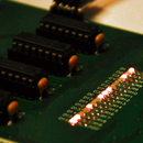
When I tested the device, the first photos came out cool, I thought I will add some of them to the instructable for you to see the development better. I took these photos with the light off so the pattern is seen better.
The blurry image shows my first test after the synchronization algorithm was in place. Unfortunately I didn't have any power supply to power up the brushless motor, I decided to take a long exposure shot of the device while slowly moving the camera to the left. The result can be seen on the image, the digits show up good enough to make me happy for the sync algorithm.
The rest of the photos were taken right before something bad happened to the base-board, it simply stopped, I forgot about the power the LDO can handle and turned up the voltage a bit higher than I should have - I lost my motor controller while making the tests. As everyone can see, this accident happened at 23:45, that's why there are no photos of the thing after this time. I will add more photos once the new PIC arrives!
I will also replace the LEDs with bigger one, maybe even through-hole types. Making them bigger and putting them closer one to the other will look better. The blue LEDs were all-right, but had higher forward voltage - couldn't drive them properly.
Step 13: Final Words


In closing (of the instructable, not of the project) I would like to thank everyone who read my instructable - I hope you enjoyed to supervise this build as I enjoyed building it. For the subscribers, and anyone interested: I am already working at another microcontroller project, it will bring my ideas into the field of PIC development boards.
If you see this as a winner, vote on it - I'll be more than grateful.
Cheerios :)

Participated in the
Microcontroller Contest

Participated in the
Make it Glow!

Participated in the
Tech Contest


