Introduction: Small - Shake Activated Water Bottle Night Light
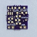
The Shake Activated Water Bottle Night Light was one of my favorite projects. The first one was DIY proof of concept. My goal here was to make it as small as possible. To do that, I had to go with a PCB, a printed circuit board. In doing so, I made the light about 1/10th of the original size.
The secret here is switching almost all the electrical parts to surface mount components. Which is where the real size savings come from.
Another size issue I wanted to address was the battery source. In the original DIY version I used a rechargeable lithium battery pack that needed a battery management and recharging board and a USB adapter. I switched all of those components in favor of using 2x 2032 coin cell batteries. A lot of space was saved, and also in the cost department too. Although the coin cell batteries are not rechargeable, their cost is a fraction of the parts I had originally used.
The size savings is great. Weight is also a huge savings factor too. Monsters and the night have no chance now!
Step 1: Gather the Tools
Soldering Iron
- A soldering iron with a finer tip would be best for SMD parts
- Solder
- Tweezers – to help with the soldering of small SMD components
- Flux (optional)
Step 2: Gather the Materials
Note that
the quantities listed are for one shake light only. Quantities would need to be multiplied by the amount of boards one would desire to build.
1x LED, Orange
2x 100k ohm pot
1x 556 timer
1x Double diode
1x Tilt switch
Step 3: Create the PCB Files With EAGLE
We will go through some of the steps to create the PCB, but this can be skipped if desired. The PCB files that were generated to have the boards made will be made available. However, this is a good exercise to go through and in doing so will be a good learning experience. In addition, if you wish to make any modifications or change the layout and board shape this step will be necessary.
Autodesk EAGLE PCB design software was used to create the Shake Light circuit boards. EAGLE is one of the most widely used PCB tools for hobbyist and professionals alike. A free version is offered which will allow you to make smaller 2 layer boards, and for reasonable price an upgrade can be purchased to make larger multilayer boards. OSH PARK, the board-house we will use to fabricate the PCBs, works very well with designs made in Eagle. There are many additional options available for you to have the boards made, but we will not go into that here.
Step 3-1: First a new project and schematic will need to be created in EAGLE. This can be done after opening Eagle under the “File” menu in the top left corner.
Step 4: With a New Schematic Window Open, We Can Begin Placing Components Down
Step 3-2: With a new schematic window open, we can begin placing components down. This can be done through the toolbar on the left hand side of the screen. The icon looks like an arrow or op amp with a + sign on it. Furthermore, by hovering your cursor over the icons, a short description of the button’s functionality will be displayed.
When selecting the “add components” button a window will be displayed with all the installed libraries of parts. By default when installing Eagle it will come with a large library of parts. In fact, all of the components used in this design are available by default in the standard EAGLE libraries. Once you have found the component you would like to use click “OK” and you will be able to place it in the schematic. Once placed in the schematic it can be moved, copied, rotated, or deleted.
Step 5: Net
Step 3-3: Once all of the components are placed they need to be connected together. This is done by choosing the “net” selection along the toolbar on the left.
Try to keep your schematic neat and organized, it is good practice and will look more professional. It will also help if you need to go back and try to debug a problem. Your finished schematic should look somewhat like the image shown below. Notes are also good to place on the schematic, they will serve as good reminders later for things that may be easily forgotten. Before moving on, one more thing I would like to note is that there is a grid available to turn on or off depending on your preference. I personally like the grid and usually have it on when putting schematics together. This can be done through the top tool bars. If you click on the matrix looking button, the grid settings will be displayed, and you can choose to turn it on and change the parameters.
Step 6: PCB Components Placed
Step 3-4: The next step for us is to get the PCB components placed and laid out. First, we will need to choose the “generate/switch to board” icon pointed to by the big red arrow. This will auto-generate a board for you.
Step 7: Arrange Board
Step 3-5: Arrange the components on the board to resemble the arrangement in the schematic if possible. Depending upon space constraints or desired board shapes and dimensions this may not be possible. We chose to go with a more unique shape for this specific project. This will give us the opportunity for more unique enclosure possibilities. Shown below is the layout, fully placed and routed. We will not go into the details on the steps of the layout as there are many thorough details on this that can be found online.
A few quick notes before moving on, when traces need to be routed to the left or right, it is good to do this through 45-degree angles. I would recommend avoiding right angles unless absolutely needed. In addition, a ground plane or ground fill is good to add. This can be easily done in EAGLE using the polygon shape and covering the board outline. One last note to mention. It is good to place ground vias throughout the PCB where there is no traces and parts placed. This will help keep all the grounding at the same potential and will also help from any ground “islands” from being isolated form the rest of the PCB.
Step 8: Generate Gerber Files for the Board-house
Go to the OSH PARK CAM jobs
page to download the 2-layer cam file. Note that you will download different files for different versions of Eagle.
Click the CAM processor icon.
Within the CAM processor window, click File -> Open -> Job… and then navigate to the cam file. Click on it to load it. Then click the “Process Job” button.
With the OSH PARK cam file loaded, the CAM Processor window will look like this. Unless you specify otherwise, EAGLE will put the Gerber files it generates in a default location. This can be less than ideal because it the save location may not be obvious and the Gerbers may be mixed with other files. Sorting the Gerbers from the other files at a location can be a real pain.
To save yourself a bit of effort, you can specify a save location for the Gerbers by clicking the “File” button pointed at by the red arrow. You will have to do this for each tab within the CAM window.
Finally, to generate the Gerber files, click the “Process Job” button.
Attached to this step are the PCB design files.
Attachments
Step 9: Order the PCBs From a Board-house
You could go anywhere to get your boards made but we prefer OSH PARK. Their prices are hard to beat and the lead times, while not the fastest, are very reasonable. All you have to do is ZIP up the Gerber files, and upload them to the OSH PARK upload page.
PCBs from Osh Park.
Step 10: Populate the PCBs With Components
First, make sure your soldering iron is hot and ready to go. Some soldering iron’s have a variable temperature setting, this can be somewhat confusing for people new to soldering. I personally like the soldering iron to be around 700 degrees Fahrenheit. This is pretty much hot enough to “get in and get out.” When an iron is placed on a pad for too long, it can cause the pad to lift off with the iron or partially become ripped up. It is best to avoid this at all cost as that can render a PCB useless and that would be the last thing you would want to happen. So, once again, the iron should be set hot enough to melt the solder quickly without having to hold it to the pad for too long.
Shown above is the PCB partially populated with the IC and a few of the caps and resistors. I chose to start from the middle of the board and work my way out. Doing this allows you to avoid already soldered down components from getting in the way. You can also work from left to right or top to bottom, but it is good to avoid randomly soldering down components. Additionally, I would recommend saving the largest components for last as they can really make working around them difficult. In this case, it would be the potentiometers, LEDs, and battery holder that were saved for last in that order.
There are a few different ways to get SMD components onto the board nicely. What was done here was placing solder on one pad with solder in one hand and an iron in the other, then using tweezers and an iron to place and solder the corresponding component to this pad. Once the solder is dried you can get to the other pad with the solder and iron.
Step 11: 3D Printed Enclosure or Bottle Cap
This step is in the gray area. What I printed wasn't a completely enclosed and water proof cap. It was simply for demonstration purposed.
I wanted to make a clear 3D print, but the material was on back order.
Notice in the 3D print that there is a single pass through hole in the center. That is to allow the LED to shine down into the bottle. In this case, the whole LED sticks through.
Attached is a Solidworks part drawing. Feel free to make changes how you see fit.
Step 12: Shake and Test
The final step would be to insert the batteries and test the Shake Light. The battery holder chosen for the design fits two CR2032 coin cell batteries which produce 6.0V nominally. There also happens to be a CR2016 battery which is 3.0V and half the physical height of the CR2032. Furthermore, the 556 timer used in the design needs a minimum of 4.5V to work properly. Therefore, two of the CR2016 (or 2x CR2032) batteries are needed to power and test this project.
With the batteries inserted and the ON/OFF switch set to the ON state, you can shake the PCB and see how the LED response. The two potentiometers used on the board can be adjusted to give different LED brightness settings and time delay settings – how long it stays on. After adjusting each to your desired settings, the PCB is complete and ready to set in a fixture of your choice.
Step 13: Upgrades and Future Changes
Using a single white LED is not a bright as I would have liked it to be.
The next version will have the following:
- 1W surface mount LED or several 5mm through hole LEDs
- Use a two sided PCB, reducing the size once again
- Potentially a return to lithium batteries in some capacity. Lithium cells can offer up more current versus other battery chemistries. A 1W LED would need it.
- Adaptation to a standard 20oz/2L soda bottle, as opposed to the off water bottle I have been using.


