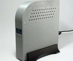
Introduction: Sous Vide Cooker With Zybo Board
The goal of this project is to convert an analog crock pot to a sous vide cooker. Sous vide is a method for cooking food in a precisely temperature-controlled water bath. The system uses a digital thermometer and PID feedback control to maintain a water bath at a precise temperature set by the user.
This project was completed for Cal Poly San Luis Obispos course CPE 439: Real Time Embedded Systems, taken in Fall 2016. It uses a Zynq-Zybo-7000 development board running FreeRTOS.
This project uses the following components:
- Zynq Zybo-7000 Development Board
- 4.5 Quart Analog Crock Pot
- DS18B20 Digital Thermometer
- Powerswitch Tail II
- Breadboard
- MPQ3904 Quad NPN Transistor (or any similar NPN transistor array)
- 3 Resistors (100 kΩ, 10 kΩ, 4.7 kΩ)
- Male to male jumper wires
- 22AWG wires
This project takes inspiration from Adafruit's Arduino powered Sous video controller:
https://learn.adafruit.com/sous-vide-powered-by-ar...
It also adapts code from Electric Imp written by Theo Habers:
Step 1: Vivado Setup
Download Vivado from Xilinx's site. This project uses version 2016.2 with the WebPack license.
After installing Vivado, create a new project. Give it a name and choose a location. On the next page select RTL project and check the box for "Do not specify sources at this time". Click next, and on the part selection page search for "xc7z010clg400-1". Select this part, click next, and then finish.
After creating a project, click on 'Create Block Design" on the left side of the screen, under IP Integrator. Leave it named design_1 and press OK. It will give you a prompt to add IP. Click this button, and search for "Zynq". Click on the option that comes up and you will add a block labelled ZYNQ7 Processing System.
Download the Zybo definition file from https://github.com/ucb-bar/fpga-zynq/tree/master/z...
Double click on the Zynq block, and click "Import XPS Settings", and import the .xml file you just downloaded.
Navigate to MIO Configuration. Under I/O Peripherals, check UART 0. In the drop down box, select MIO 10 .. 11. This enables the UART used to communicate with the digital thermometer, and specifies that it will use MIO pins 10 and 11. Also under I/O Peripherals, open GPIO and check GPIO MIO.
Finally enable Timer 0 and Watchdog under Application Processor Unit. Press OK.
Step 2: Adding GPIO Blocks
Next GPIO blocks need to be added. These blocks allow for communication between the FPGA and processor.
Right click on some empty space in the block diagram. Click Add IP and search for gpio. Select the option that comes up. Under GPIO, check the box for All Inputs and set GPIO width to 8. Also check Enable Dual Channel. Under GPIO 2, check All Outputs and set the width to 8. Press OK.
Now repeat this process to create two more GPIO blocks. The second block you create will only have one channel consisting of all outputs and a width of 25. The third block will have two channels: the first with 4 outputs and the second with 4 inputs.
After creating three GPIO blocks, click on the prompt for "Run Block Automation". Press OK on the window that pops up.
Next click on the prompt for "Run Connection Automation". Under each gpio, select the box for S_AXI.
Next, notice that each GPIO block has one or two connections on the right side labelled GPIO or GPIO2. For each connection, double click on the adjacent double vertical bars and click on Make External. You will see several new connections show up. Starting with channel 1 of the axi_gpio_0 block, rename these connections to the following:
TEMP_OUT, TEMP_ERROR, PID_CONTROL, LEDS, SWITCHES
Finally, right click on some empty space and click Create Port. Name it R_CLOCK and change it to an Output. Press OK. Hover your mouse over the port until you see a pencil icon. Click and drag towards the FCLK_CLK0 line to connect the port.
Your block design is now finished! It should look something like the above block diagram image.
Step 3: Generate HDL Wrapper
Click on the Sources frame. Right click on design_1 under Design_Sources and click Create HDL Wrapper. Select "Copy generate wrapper to allow user edits" and press OK. This will create a verilog file. Replace this file with the contents of the edited file design_1_wrapper.v file included below.
Next we need to add a second HDL file for the PID controller. First download the file called pid.sv. Go to File->Add Sources and select "Add or create design sources". On the next screen click on Add Files and select the pid.sv file. Check the box for "Copy sources into project". Click Finish.
Finally we need to add a constraints file. Download the file called ZYBO_Master.xdc. Click File-Add Sources. This time select "Add or create constraints". Add the .xdc file and click Finish. This file maps the inputs and outputs from our wrapper to pins on the Zybo board.
Now your design hierarchy should resemble the above image.
Step 4: Generate Bitstream and Export Hardware
Click on Generate Bitstream on the leftmost pane, under "Program and Debug". This will also run synthesis and implementation. This process will take a few minutes. Wait until you see the "write_bitstream Complete" towards the top right before proceeding. A window will also pop up saying "Bitstream Generation Completed". Click cancel unless you're interested in viewing the implemented design.
Click on File -> Export -> Export Hardware. Check the box for "Include bitstream" and press OK.
We are now finished with our Vivado work. Click File -> Launch SDK and press OK.
Step 5: Creating a Board Support Package
After the SDK launches, go to File -> New -> Board Support Package. Leave the default settings and click Finish. Another window will pop up. Check the box next to lwip141, then press OK.
Step 6: Import FreeRTOS
Download the latest version of FreeRTOS from Sourceforge: https://sourceforge.net/projects/freertos/files/la...
Extract the downloaded file into your project directory.
In the SDK click File -> Import. Under General select "Existing Projects into Workspace" and press Next. For the root directory navigate to FreeRTOS/Demo/CORTEX_A9_Zynq_ZC702/ and select the RTOSDemo folder. Press Finish.
Next we need to change the referenced BSP for FreeRTOS. Right click on the RTOSDemo folder, click Change Referenced BSP and select the BSP we just created.
If you are unable to pick this BSP, try creating a second identical BSP using the same process as the first one. Then right click on RTOSDemo, select Properties, go to Project Preferences and check the two BSPs you created. Now try to change the referenced BSP and you should be able to select the second BSP you created. If you would like, you can then delete the first BSP since it is not being used.
Step 7: Modify FreeRTOS Code
The FreeRTOS demo includes three examples. This project modifies the Blinky Demo to run our own code. First open the main.c file in the SDK located under RTOSDemo/src/. Scroll down to #define mainSELECTED_APPLICATION and change the value from 1 to 0. This causes the blinky example to be run. Also, find the line vParTestToggleLED( mainCHECK_LED ); and comment it out. This will prevent an error later since we will be getting rid of this function.
Next open main_blinky.c under the Blinky_Demo folder. Replace this code with the included main_blinky.c file. Do the same for ParTest.c located in RTOSDemo/src/, and for ParTest.h in RTOSDemo/src/Full_Demo/Standard-Demo-Tasks/include/.
Take note of lines 112-114 in ParTest.c. These lines define the coefficients used for PID control. These values need to be modified to tune the PID controller.
Step 8: Setup Debug Configuration
Next we will prepare a debug configuration to run the code. Right click on RTOSDemo and select Debug As -> Debug Configurations. Right click on Xilinx C/C++ Application (System Debugger) and click on New. Under the Target Setup tab, select Reset Entire System and Program FPGA. Click Apply, then Close. Before actually running the Debug Configuration, the hardware needs to be setup.
You will also need to install the correct drivers for the Zybo board before running the program.
Step 9: Hardware Setup
The hardware setup has several parts. The DS18B20 digital thermometer measures the temperature of the crock pot water bath. The DS18B20 uses 1-Wire protocol. Rather than writing 1-Wire specific drivers, this project uses the Zybo board's UART drivers to read values from the thermometer. Interfacing to a 1-Wire device using UART requires an open collector buffer.
Finally the Powerswitch Tail II controls power delivered to the crock pot. The Zybo board controls the relay's operation using time proportional pin. Time proportional output varies the amount of power delivered by the relay using pulses with variable widths, similar to PWM. However, the pulses occur at a much lower frequency of 0.1 Hz.
Step 10: Build the Open Collector Buffer
Construct the above open collector buffer circuit on the breadboard using the NPN transitor array and resistors. This circuit allows the digital thermometer, which uses 1-Wire protocol to be driven by the Zybo board's UART. The TX and RX lines connect to MIO pins 10 and 11 on the Zybo board, which correspond to Pmod pins JF2 and JF3. VCC corresponds to the 3.3 volts supplied by the Zybo board. This voltage can be drawn from pins JF6 or JF12 from the same Pmod header. Similarly, the GND can be connected to pins JF5 or JF11. The power and ground pins on the DS18B20 thermometer must also be connected to these rails.
Step 11: Connect the Powerswitch Tail II
Connect the Powerswitch Tail II to the Zybo board using the +in and -in terminals. The +in terminal connects to MIO 9 on the Zybo, which corresponds to pin JF8. The -in terminal connects to the GND rail.
Connect wires to the Powerswitch terminals by stripping solid core wires approximately 1/4 inch and then using a flathead screwdriver to secure them to the relay.
The male end of the Powerswitch Tail connects to a 120 Volt wall outlet. The female end connects to the analog crock pot's power plug.
Step 12: Operating the Cooker
After completing all the previous steps, you are now ready to operate the cooker.
Fill about 3/4 of the crock pot with water, then place the thermometer inside. On some crock pots, you may be able to unscrew the lid's handle and insert the thermometer through the hole.
Run the RTOSDemo program on the Zybo board by clicking on Run -> Debug in the SDK.
To set the temperature maintained by the device, use the four switches located on the Zybo board. The four switches use a binary weighting. If all the switches are off, the set temperature will be 25°C. Toggling the rightmost switch will increase the set temperature by 4°. The second switch will increase it by 8°. The third will increase by 16°, and the last by 32°. This allows for any temperature to be set between 25°C and 85°C.
The LED labelled LED4 on the Zybo board will turn on when the measured temperature is within 2°C, indicating that the water bath is ready to use.
There are many resources available online on sous vide cooking. Most recipes can be completed using this project. Make sure to exercise proper food safety and properly seal any foods cooked using this device.
Step 13: PID Tuning
The coefficient values used for this project's PID controller are set in ParTest.c, on lines 112-114. By default, the derivative and integral coefficients are set to zero, so the system relies on proportional control. In order to tune the system and improve it's response, these coefficients must be adjusted. The best values for a given system depend upon its physical properties, and will vary based on factors like the crock pot being used. There are many methods for tuning a PID system. For example, the Ziegler-Nichols method, which starts by adjusting proportional gain to achieve stable oscillations:


