Introduction: 3 Axis EasyDriver PCB


I am in the design and testing phase of creating my first CNC Mill.
I've got my overall design mostly done and I'm in the build stage for the CNC Mill body and there are loads of instructables about them (yes, I will add to the overall pantheon of mill design and build instructables). I thought that it would be a good idea to write a couple of instructables focusing on each of the parts of a 3-Axis CNC Mill. In this instructable, I will be focusing on the construction of a board for the three controllers.
In this design, I am using three EasyDriver version 4.4 modules.
My goal is to fabricate a circuit board that houses the three EasyDriver modules with a simple socket design allowing me to pull out and push in modules, should the need arise to replace any of them.
The board will service the modules power and signal needs with copper traces as much as possible, to reduce the rats nest of wires and to allow easier heat management.
I'm designing the circuit board using Fritzing and I will be using the laser printer toner transfer method of transferring the design onto the board. I'm also using acid to etch the board.
The above image shows the overall design and includes the EasyDriver modules in the silk. As the modules will plug in to some female header pins, I'm not including the silk outline for the EasyDriver modules in the printed design.
This instructable will be in two parts and with as much detail and information as I can provide.
Step 1: Parts - or Bill of Materials

As this circuit is essentially a carrier board, there are very few parts ... and all of them are passive. The Bill of Materials comes out very light indeed:
- 17 x Generic female header - 2 pins
- 6 x Generic female header - 4 pins
- 3 x Generic female header - 3 pins
- 1 x 2 channel DIP switch
- 3 x EasyDriver v4.4
The main features of this board are:
- Sockets for each EasyDriver (15 pins per module);
- Break-out sockets for the Step Motor connections;
- Break-out sockets for Step and Direction connections (to Arduino);
- 2 bit DIP switch for selecting the micro-switch level;
- 2 holes per EasyDriver for securing the module to the board;
- 5V fan socket; and
- 12V input socket
Step 2: More Info on the "Features"
The DIP switch connects the three MS1 connectors together and then (via the switch) to Ground, likewise, the three MS2 connectors are joined (via the switch) to Ground. This provides selection of High or Low for MS1/MS2, giving a switchable micro-step selection as per the design of the EasyDriver (HH, HL, LH, LL). By default the EasyDriver is set to HH for 8 micro-steps. If your step motor is like the ones that I've ordered with 1.8 degrees per step then you have:
(360 degrees ÷ 1.8 = 200 steps) x 8 micro-steps = 1,600 steps per revolution
when MS1=H and MS2=H ... in case you wanted to know ...
I have ganged the MS1 and MS2 together on the basis that I would expect to use the same number of microsteps for each axis.
Each EasyDriver provides a 5V output, the carrier board breaks the 5V out to connect to a 5V fan. In this design, I'm manufacturing an aluminium heat sink that has a fan on top to help dissipate the heat that the EasyDriver will produce, the consumption of some of the power by the fan is also intended to reduce the amount of energy spent as heat (but not much).
Each Axis has a pair of break out female pin headers that can be used to connect the carrier board to an Arduino.
The attached PDFs are etchable PDF. If you use these you must print them without scaling otherwise the size will not match the parts.
The intention is to connect an ATX power supply (12V) to the Arduino and connect the Arduino to the carrier board via the VIN socket of the Arduino. The Arduino get's to steal some power and pass the rest on to the carrier board. The Arduino also connects GND to the carrier board.


Step 3: Transfer

The Toner Transfer Method is about using the toner of your laser printer as a resist on a copper clad PCB.
This method is achieved by printing out your circuit design onto plain paper using a laser printer. You can improve your chance of success by increasing the print density on your printer (next page).
When you have printed your design, cut it out so that it will fit on your blank copper clad PCB with the printed side down (touching the copper).
You will need a domestic iron, a flat wooden surface (I bought a bamboo cutting board for this purpose) and a container with hot water in it to immerse the board after cooking. You want hot water so that you don't give the board thermal shock after heating it to > 100 degrees with the iron.
Using a domestic iron set to it's hottest setting (typically, that's on "Cotton"), rub the iron over the paper pressing down firmly.
The easiest approach that I have found is to iron a corner of the board first, this will heat the toner making it stick to the copper and, effectively, gluing the paper to the copper. Simply hold the paper in position with your free hand while ironing the corner down. Of course, the corner that you iron down must have some toner on it ... otherwise there will be nothing to "glue" with.
When one corner is "glued" you can iron the rest of the board down (remembering to take your hand off so that you don't burn it).
I rub the iron onto the board for about a minute, turn it 90 degrees clockwise, and repeat until I have ironed and turned 4 times. Then I look at the board and make sure that there aren't any "flat" spots, that is spots that the iron hasn't heated. For them, I use the tip of the iron and rub it until it looks as cooked as the rest of the board.
When the board is completely ironed, immerse the board in the hot water and let it soak until the water is about body temperature
Next, run the board under the tap and rub the soaked paper off the board.
You may find parts of the design that haven't transferred properly. I go over the entire board with a Staedtler Lumucolor (black) waterproof pen retracing the design. From experience, I've found that these pens deposit an ink that is a reasonable acid resist. They are not good enough by themselves, but they do improve the acid resistance of the toner somewhat.
With the last traces of paper removed from the copper board, you are ready to acid etch.
Step 4: Printer Settings for Toner Transfer


But first ... a word on printer settings for improving your chance of a decent transfer image.
I've got a Brother HL-2130 printer and I'm using Windows 7 Home Professional ... so you will probably have to find your own way around in case your settings aren't the same as mine.
I open the design PDF and change the Auto Size Adjustment settings to make sure that my image is going to be printed out without being rescaled.
Because I am miserly, I also print multiple copies of the image on the page, so that I can get more than one transfer if needed. On a side note ... I keep the remaining copies in a folder in my filing cabinet if I want to make more of the same circuit.
With my printer, you get to the print density settings by going into Advanced > Other Print Options. Uncheck the Printer Default option and wind the printer density all the way up to darkest.
These settings result in a good level of toner on the paper, ready to be transferred to the circuit board.
Step 5: Acid Etching


NOTE ... this is NOT a safe procedure to be conducted by children or childish people ... or people who think that acid is a toy. You must take EVERY precaution to protect yourself and your environment from accidental acid spills, splashes and fumes. You are responsible for your safety and the safety of those around you.
Acid etching is a fairly simple process, but carries a risk and some disposal responsibilities with it.
Okay, I'm leaving the moral/ethical/safety issues in your hands and completely absolving myself of any responsibility.
Mix your acid by placing 2 parts of Hydrogen Peroxide into an acid resistant flat bottomed container. At the moment, I'm using an old plastic butter container. It's starting to pit a little, so I'm going to try to find another acid resistant container. Your container should be slightly larger than your board, so that you don't need to mix so much up.
Next, place 1 part Hydrochloric Acid into the container.
Remember to ALWAYS add Acid to Peroxide. If you do it the other way around, you are staring down the barrel of a fairly significant level of stupid. DO NOT DO IT.
Normally, when you add your acid to the peroxide, the solution turns green. The acid that I'm using seems to have some ferric chloride in it, so it turns a reddy brown. This doesn't affect the etch, so if yours is red/brown rather than green ... don't worry.
I hold the acid bath carefully in two hands and tip it slightly from side to side to agitate the solution. This has the effect of sluicing the copper away from the board and allowing the solution to mix while it is etching. This method is much faster than putting the acid bath down and leaving it to it's own devices. I usually have a board etched in @ 5 - 10 minutes, compared with 10 - 20 minutes without agitation.
In the third bath image, you can see that the substrata as the acid has eaten the copper away. In the 4th, the copper is disappearing well.
When the copper is completely gone and you are only left with the black design on the substrate, it's time to take the board out of the acid and give it a cleansing bath of salty water. The salt will slack the acid, stopping it from reacting with the metal.
Sometimes, the acid will keep on etching after the board has been removed from the bath, so you want to make sure that you have neutralized the acid (with an alkaline ... salt) to stop the reaction.
Once you have thoroughly rinsed the board and dried it ... you have a board that's ready to clean up.
Step 6: Clean and Inspect


Cleaning the toner off the copper is a simple process of wiping the board down with a tissue that has been dipped in acetone.
The acetone melts toner (and the Lumocolor ink) allowing the tissue to soak it up.
By this stage, you have revealed your cool new PCB ... all ready to be drilled and populated ... or is it?
There are two ways that you can test your board to find all of the places where the toner wasn't good enough, the Lumocolor didn't deposit enough ink, where the acid undercut the resist and ate it from beneath ... where, frankly, you didn't notice a pad or trace that wasn't properly prepared ...
This happens all the time with the acid etch method, so don't beat yourself up over it ... this is a hobby, not a laboratory, so, meh, whatevs
The two ways that you can test your board are:
Visually.
Look at the board under a microscope, under a magnifying glass, with your perfect 20/20 vision. You are looking for parts of the trace where any of the above reasons have come to fruition and you can "see" that there is a break in the trace.
Image 7 above, is a part of the board where I have a 2-bit dip switch, there is an apparent scratch in the copper that seems to cut the pads off from the traces.
Image 8 shows a section of the board where it looks like I've been trying to make a circuit board out of cheese.
A visual inspection allows you to identify parts of the board that may be a problem.
Multimeter
A multimeter switched to "continuity" will allow you to pass a current through the trace from the anode to the cathode. When the current can pass through, it sounds a squeak. When no current can pass through ... you get no squeak. Bear in mind that this does not tell you that enough current is getting through, only that some can. The parts of the trace that are very thin on path will be "resisting" current ... you can use your multimeter on Ohm-meter mode to find out how resistant the thin path is.
Over the parts of my circuit, I'm registering 1.2 - 1.4 ohms resistance, this is a tolerable amount, so I'm not too unhappy about the circuit traces, nevertheless, I will solder over the areas of the board where the traces appear "dodgey".
So you've found some problems ... now what?
There are a couple of ways to fix the problem and it will depend on how much of a problem you have.
- Start from scratch ... throw the board away and start again.
- Draw over the break with an (expensive) ink that conducts electricity, such as a silver ink pen (not just coloured silver, but with silver in it).
- Lay a small piece of cut-off wire (from a resistor, capacitor, LED ... anything that you've trimmed in a previous project. I keep a drawer in my parts cabinet for these and clear it out once in a while) and solder it over the gap to make a bridge.
- Solder a blob over the bridge or the area of poor conductivity. Soldering over a bridge is a pain because the solder will naturally shrink away from the gap .... you may need a lot of solder to bridge.
Any of these techniques may work, but they will depend on your patience, your resources and the nature of the problem.
Step 7: What's Next?

Well ... I've taken this instructable as far as I can for now.
I am waiting for components to arrive from EBay (female header pins and EasyDriver) so I can't show you the populated board.
I'm also waiting for a new PCB drill, so I can't drill the board.
I will make a second part to this instructable when I've received all of the other bits that I need so that I can show you the completed board including drilling, populating and testing.
Please come back and follow the next installment of this instructable.
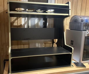
Step 8: Carrier Board Population


Well, I've received most of the components that I needed to make the carrier board for the three Easy Driver modules. There was a mix-up with the 4 pin headers (I ordered 10 and received 5 x 4 Pin Headers and 5 x 5 Pin Headers) and I'm waiting for some more components (grumph).
I've also tweaked the board design slightly ... the PDF files earlier in this instructable have been updated accordingly.
I've removed the 5V output from both the X and Y Axis and put a diode between the 5V output and the fan on the Z Axis. This was done to protect the Easy Driver from any reverse bias current (not likely, but better to be safe). This simplifies the design a little and makes it a lot easier to make (less to solder).
I started by soldering in the two jumpers in the middle of the board, and then the 1N4001 diode. Once these were in place, I soldered in the 2 bit dip switch, then all of the 2 pin headers, 3 pin headers and finally the 4 pin headers.
I decided to forgo the output 4 pin headers on the Z Axis for now (while I wait for my replacement order to arrive) so that I can plug in the Easy Drivers (when they arrive) and power the circuit up. The missing output will not have any significant impact on testing the circuit and I can wait until I test the Z Axis.
Yesterday, a friend gave me his old PCB drill that he isn't using anymore (a Maxicraft 20000), this certainly made drilling the board a breeze compared to using a pin vice! The nice thing about the PCB drill is that it came with 9-30V a power supply ... now that's going to be very useful indeed.
Step 9: EasyDriver V4.4 Arrive


Today, the EasyDrivers arrived (yay!).
I broke the header pins into their smaller sizes (1x4, 1x3, and 4x2) and placed them in the header sockets on the carrier board and then fitted the EasyDriver boards (x3) onto their pins.
With the EasyDriver boards sitting on their pins, I then soldered the pins in-situ so that I know that the pins will fit nicely into the carrier board.
After soldering, I tested taking the EasyDriver boards out and reconnecting them ... works a charm.
Next, I tested the carrier and EasyDrivers with 12 volt power supplied, the indicator lights all lit up on the EasyDriver boards, so that's just fine.
I've taken the IN4004 diode out of the circuit and replaced it with a 0 Ohm resistor (aka jumper)
The next tests that I need to run on this circuit are:
- 5V output power supply (the cooling fan) (works)
- Connecting the motors
- Connecting the Arduino
- Running the sketch
I'll get back to that, now it's time to do some overtime for work.
Step 10: Connect EasyDriver Carrier Board to Arduino

Finally, connect the EasyDriver board to the Arduino. For this I've connected the X-Axis to pins 12 and 13, Y-Axis to pins 10 and 11 and the Z-Axis to pins 8 and 9 of the Arduino. 12, 10 and 8 are connected to the Step Pin and 13, 11 and 9 are Direction pins.
Programming the Arduino is still a work in progress. I'd like to get the three axis working together, and for that I'll probably have to have three microprocessors being controlled by the Arduino, that is 3 x ATTiny chips controlling the step and direction of the three axis with the Arduino controlling the three ATTiny chips.
For now, connecting the Arduino to the EasyDriver boards and controlling the step motors is done using the sketch that I've added here. The sketch simply rotates each of the motor shafts clockwise and anti-clockwise, repeatedly and is intended only to test the overall circuit.
Through this article, I've learned a bit about step motors and the Arduino. Hopefully, you can get some benefit from this article too.