Introduction: Getting Started With Xilinx Fpga


Field Programmable Gate Arrays (FPGAs) are semiconductor devices that are based on a matrix of configurable logic blocks (CLBs) connected via programmable interconnects. In this tutorial, I'm going to explain how to program Xilinx FPGAs using a Xilinx Platform Cable USB and ISC software. For this, you have to prepare following items:
1. XC6SLX9 Starter Board, Xilinx Spartan 6 FPGA -
This board includes a target FPGA device (Spartern-6, XC6SLX9) and some other necessary circuitry and peripherals to support the running of the device.
(You can buy from this board from ebay: http://www.ebay.com/itm/XC6SLX9-Starter-Board-Xil...
2. Xilinx Platform USB Download Cable Jtag Programmer for FPGA -
This is a programming tool to download an configuration file generated by ISE WebPACK to the internal SRAM of the target FPGA device or an external non-volatile memory.
(ebay link: http://www.ebay.com/itm/Xilinx-Platform-USB-Downl... )
3. ISE webpack software -
We use HDL( Hardware Description Language ) code like Verilog or VHDL to describe a digital circuit, code must be compiled and ultimately implemented into a circuit layout that can be programmed to FPGA device. ISE WebPACK Design Software is an fully integrated tool for this purpose provided by Xilinx.
(You can download from Xilinx website: http://www.xilinx.com/products/design-tools/ise-d... )
Step 1: Download and Install ISE WebPACK Design Software


Xilinx provides a free IDE software named ISE WebPACK for beginners. It's a IDE for FPGA design using HDL simulation and implementation. You can download ISE WebPACK Design Software webpage for details and download it to your PC. In here I installed version 14.1.
Please follow the instructions on the images.
Step 2: Setup Xilinx Platform Cable
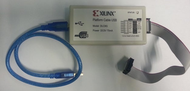

A download cable is needed to program the configuration file to the target FPGA device. Xilinx provides USB download cable or you can buy a clone version from ebay. A USB driver software is needed for this cable. It's integrated with the ISE WebPACK Design Software and has been installed in the previous installation process. If driver software is properly installed, the cable named Xilinx USB Cable will appear in the Device Manager list.
Step 3: Create Your First FPGA Project


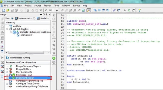
This section I will guide you through the process of creating a simple FPGA project using VHDL. I build a simple AND gate using two input switches and one output LED. Finally, the program file will be downloaded to the target device on XC6SLX9 Starter Board.
Double-click ISE Project Navigator icon to start the IDE.
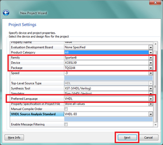
Step 1 - Select File -> New Project... The New Project Wizard appears.
Step 3 - step 9 - Do as shown in figures
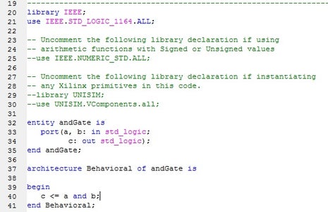
Step 10 - Write AND Gate VHDL program as follows.
entity led1 is
port(a, b: in std_logic; c: out std_logic ); end led1;
architecture Behavioral of led1 is
begin
c <= a and b;
end Behavioral;
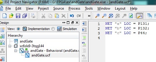
Step 11 - Then we have to map the actual port pins to program symbols. This can be done by creating ucf file as shown in step 11,12 and 13. On ucf file, write following program to map a,b,c to P131, P132 and P44 respectively.
Step 14 - Double click on "Implement Design"
Step 4: Program Your FPGA


Now we have to program the generated bit file to FPGA. I will explain this process in several steps by figures as previously.
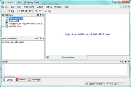
Step 01: go to "tools -> iMPACT" and then it will open the iMPACT window as shown in figure.
Step 02: Then double click on "Boundry Scan".
Step 03: Then right click on the work space and select "Add Xilinx device" option.
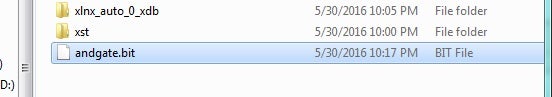
Step 04: Then open the "andGate.bit" file.
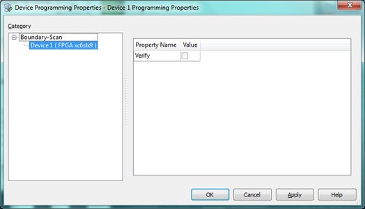
Step 06: Then right click on Xilinx green color chip and select the "program" option.
After finishing the program it will notify by the blue color box as shown in the last figure.
Then press the BTN2 (P132) and BTN3 (P131) in same time and observe the LED (P44) status.
Step 5: Download the Program to SPI Flash


In the previous steps, the configuration file is downloaded to the SRAM of the target device. As we know, SRAM is a kind of volatile memory, that means data stored in SRAM will be lost when power is removed. The XC6SLX9 Starter Board has a non-volatile SPI flash( W25Q64FV ) to store the configuration file. Data will be automatically loaded into the SRAM of FPGA device during power up. The following steps will show you how to generate a PROM file and program it to the SPI flash.
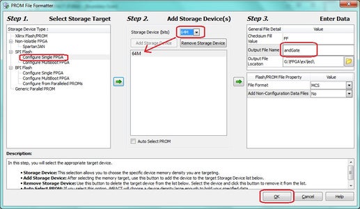
step 01: Double click on "Create PROM File"
step 02: Then configure the following settings on "prom file formatter" window as shown in figure and click ok.
step 05: Right click on Xilinx chip and select "Add SPI/BPI Flash" option.
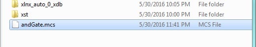
step 06: Browse for andGate.mcs file and open it.
step 07: Select SPI Flash chip model. In this case chip model is W25Q64FV which is having 64M memory.
step 08: Then right click on FLASH chip and program the flash device.
Then you can check this with your starter board by power off and then on.
Enjoy with FPGA programming !!
Download complete program from below:
Attachments


Participated in the
Automation Contest 2016

Participated in the
First Time Author Contest 2016