

Introduction: Simulating Designing of Circuits+PCB on Proteus


This is a step by step instructable for Engineers and hobbyist. In this instructable I will discuss about circuit simulations & PCB designing on Proteus 8, at the end I will also discuss about etching of electric circuits within 5 minutes.
With the help of this instructable you can make single layer auto+manual routing double layer auto and manual PCB routing. You would be able to make very small size PCB of large circuits.
Step 1: Installing Proteus 8.0
Step 2: Getting Started

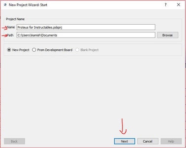
When you launch Prteus click on New Project or press CTRL+N. A new window called New Project Wizard appears
- Start
There you can change the Name and Path of the project after setting click Next
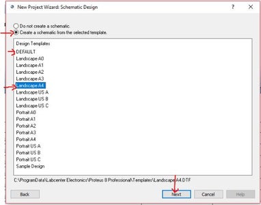
- Schematic Design
Now you need to Mark Create a schematic from the selected template then you can either select Default or you can select any templates size normally we select landscape A4, by selecting the Landscape A4 you will have a schematic window as shown in the picture 4
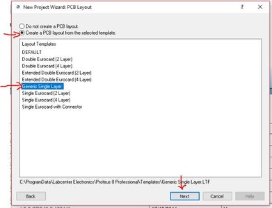
- PCB Layout
If you do not want PCB design just click Next otherwise Mark on create a schematic from the selected template, now you can select Generic single layer or any other layer of your requirement and then click Next, by selecting single layerif you do auto-routing then the software will do only single layer routing(bottom) if you select default and then upon selecting auto-routing the software would double layer(top & bottom layer routing).
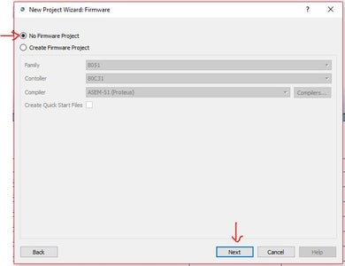
- Firmware
Normally we select No firmware Project, but if we require to work with microcontrollers like 8051, Arduino we select Creat Firmware Project, and select the options accordingly, if anybody wants to know about that just write down a comment, I would guide for that.
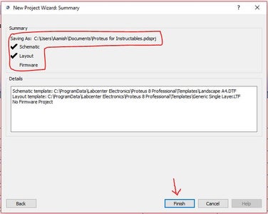
- Summary
Here you can check the selected options and click Finish.
Step 3: Placing the Components


A black colored window would appear that is PCB layout tab, you can switch the tab to schematic capture
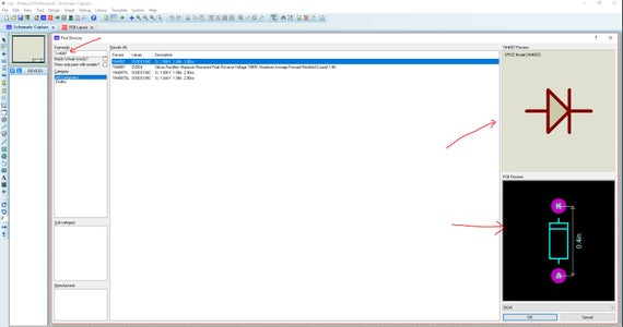
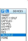
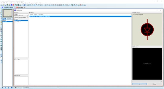
Click on P button it stands for place, a new window would appear, In this window you can search for the components by typing exact names like 1n4007(diode) or simply type diode but if you want to make PCB you have to check that your selected component has a PCB design which is shown in PCB preview. Double click the required component and it would appear in your devices and search for other components and place them all in your devices section, some of the components might not have the PCB previews but we can add the PCB layout of them(mentioned later).
Tips:
- for electrolytic capacitors just tzpe cap-elec
- for ceramic capacitor type cap
- for resistor type res
- for AC source type VSINE
Sometimes you may have different package but you are selecting another component you need to select appropriate PCB as described here for potentiometer(variable resistor) there are many kinds of potentiometer available in market so you need to first check what is available for your then you can select appropriate design, I have mentioned here some of the potentiometers.
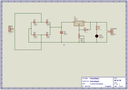
Step 4: Making the Schemetic


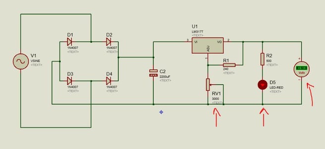
for this tutorial I designed a Variable Power Supply
- Make sure you selected the little diode button
- select any component as I clicked 1n4007 from devices section by clicking them once, then click in the area provided for drawing the circuit now the component is available to be place anyzhere, to place click again. If you want another 1N4007 just click again as many times as you want. similarly place all the components
- to join the components with each other click on one end of a component, a line would start, you can click on the other components where you want it to join like in the picture. similarly complete your circuit diagram.
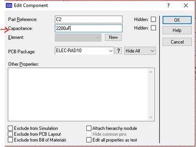
- To change the values of components(resistors, capacitors) double click on the component and change it.
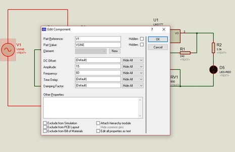
- Similarly change the value of VSINE by double clicking it. As it is AC you need to add frequency and voltage value as mentioned at output terminals of transformer.
- To add a voltmeter click on the meter icon and select DC VOLTMETER then click where ever you want to place it connect it by wires(lines) if necessary
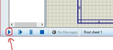
- To check the circuit click on the play icon on bottom left of the proteus.
- I have attached last two pictures by changing the value of variable resistor check the output voltage.
- At this step we have simulated our circuit and verified it on Proteus you need to save this file for later purposes
Step 5: Preparation for PCB Design

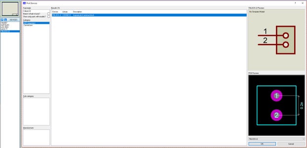


As you know we can not place VSINE or Transformer on the PCB board we need to add a block which is called as TBLOCK-I2 it is a two terminal connector at which we will connect our output terminals of the transformer similarly for the voltmeter we are going to put the same terminal block.
For this purpose we will replace VSINE and voltmeter with terminal block (TBLOCK)
Now only remaining component is LED who's PCB footprint is missing so we need to add the PCB footprint of LED for that purpose double click the LED click on the question mark a new window named packages would appear type LED and double-click LED now and the PCB package you can see there would be written LED at the end.
You can rename the terminal blocks by input and output or whatever you like
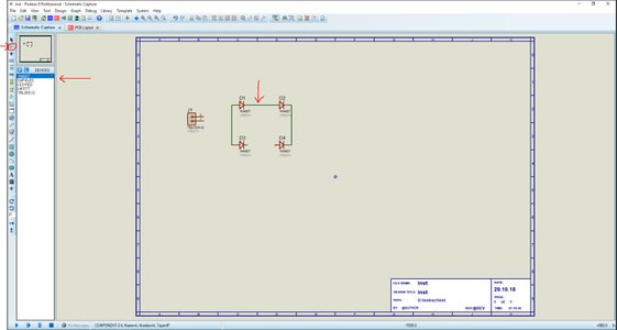
The schematic is ready for PCB designing
Step 6: PCB Desiging


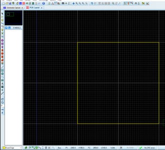
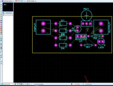


Board Edge (Border or Size)
- Click on the PCB layout tab then zoom in to upper left corner as shown in pictures this block is 1x1 cm in area
- Now from the left toolbar click on the Square button and from the bottom toolbar select Board Edge.
- Draw a rectangle of any size by clicking anywhere inside the blue area of the PCB window, as you can see I have drawn a 2 x 2 cm² block. This is the size of your PCB you can change it by hoovering your mouse pointer at any corner off this Block. As I have also changed it after completing the design.
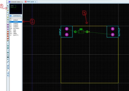
- Now click on the small diode icon which indicate that component lists. Select the component and then click inside the yellow Square to place it
- When you would be placing a component you will see green lines which indicates the connection of one point to the other point and the Yellow arrow head which indicates that this component is to join with this terminal of the other component. Place the components wherever you like keep in mind that you choose simple and easy path which is indicated by the green lines. After placing all the components you can adjust the yellow rectangle
- Make sure there are no DRC errors on the bottom status bar, DRC error appears when there is an overlapping of a terminal with other terminals or with board edge.
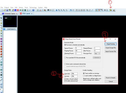
Auto-Routing
- Click on the routing button from left toolbar as described in picture then double click default, change the default width to 20th or 25th (this is the thickness of your PCB routing) and click OK
- Now click on the second last icon (Auto-Router) and check the Wire-Grid and Via-Grid it should be more than 15 other wise soldering would be difficult in close connections. then click Begin Routing
- After routing make sure there are no CRC errors, in case there is an error there would be a connection missing press CTRL+Z and re-arrange that component and start routing again.
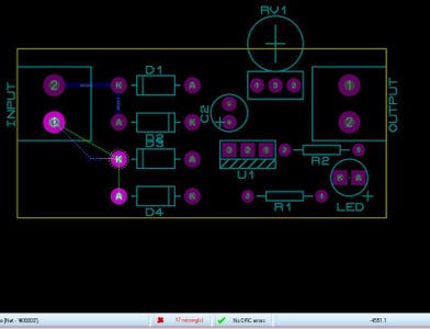
Manual-Routing
- Click on the routing button from left toolbar as described in picture then double click default, change the default width to 20th or 25th (this is the thickness of your PCB routing) and click OK
- Click on any terminal the point that terminal wants to connect would be highlighted just click on that highlighted terminal same as we did while making the schematic. Make all the connections you would notice that whenever you are making the connection the CRC errors would be reduced after all the connections there would be no CRC error.
Note : After Routing (Auto or Manual) just make sure there are no errors
Additional Step
If you want to make your PCB design more professional click on tools then the second last item name power plan generator Just click ok and see what happens with your PCB design
Step 7: 3D View


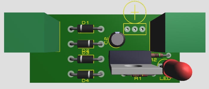

Proteus offer to students a 3D visualisation tool you can see your circuit in 3D which is quite awesome
Step 8: Printing Out PCB for Etching (Toner Transfer Method)


For etching you need to print the PCB layout on a glossy sheet from a laser printer
For printing the PCB layout there are two methods
- Go to output click on export graphics then click on export Adobe PDF file in this method you will save the PCB layout as a PDF file and dialog box will open from this box only select the bottom copper and the Board Edge and un-check everything else and click OK. You need to check the actual size printing option while printing from a adobe or any other PDF viewer.
- Go to output click on print layout, a dialog box will appear only check bottom copper and board Edge adjust the PCB as shown in the print preview you can print it anywhere on the page and click OK.
Step 9: Toner Transfer Method
- Cut the PCB sheet with scale and paper knife you can watch a YouTube video about how to cut acrylic sheet the same yqz you can cut the PCB sheet
- Take the glossy paper which has a print of your PCB layout place the printed area on the copper side of the PCB sheet it is recommended to use a scotch tape to hold it properly
- Use electric iron to transfer ink from glossy sheet to your PCB board it will take less than 5 minutes to transfer the glossy sheet, it has to stick properly on the PCB board like a sticker after 5 to 7 minutes check from one corner gently if the ink has been pasted on the PCB board. If not iron more for some time gently.
- Remove the glossy sheet from your PCB board under warm water check if there are any paper particles stuck on new PCB board if there are particles remove them by scratching them with a sandpaper
- Dry the PCB board with a tissue paper and check if they are proper markings you can check it by taking a look on your computer the PCB design should be printed on the PCB board if there are some missed printing you can mark those points with a permanent black marker
Step 10: Etching
- Take a pot or a flat bottom bowl of the size a little bigger than your PCB board
- Place the PCB me in bowl and add 1 to 2 tablespoons of powdered ferric chloride on the upper surface of the PCB
- Boil one glass of water and pour a small amount of water on the PCB containing ferric chloride the solution should be concentrated do not dilute the ferric chloride solution.
- Gently Shake the bowl if the solution is concentrated and the water is super hot the etching would not take more than 3 minutes I have even done it with in one minute.
- You would notice that all the copper is removed expect the black markered/printed area.
- clean the board with water and nail polish remover to remove the printings.
- your PCB is finally etched.
- take extra precautions while etching with hot water, the ferric chloride leaves very dirty stain on clothes.
I want to apologize that I could not show you the etching process step by step. But if you feel any problems leave a comment.

Participated in the
Electronics Tips & Tricks Challenge


