

Introduction: GoldFish - a Smart Fish Tank Controller


Get cozy.. the instructable you’re about to read is something I have been working on for a year and a half (mostly during the night and weekends) so this read might be a bit longer than one would expect. Though there is a tremendous amount of work in this project already, there is still room for improvement. If you have ideas that can make this home automation tool better, please let me know!
Step 1: Motivation and Short Description
The motivation came when a friend started talking about a small aquarium automation tool he built with Arduino. We both believed that through his knowledge in fish, plants, aquariums and electronics, plus my knowledge in embedded systems, electronics and programming we can make a great gadget that can help aquarium enthusiasts spend more time with aspects they like most, leaving the lights, filter, skimmer and others to be switched automatically through a predefined schedule. My very first tries were Arduino based. My antipathy towards the Arduino quickly resurfaced as the software started to become more and more unstable until the point where two consecutive flashings resulted in completely different behavior. When I read that using more than 75% of RAM can result in such instability, I decided to take matters into my own hands and make the main and control boards myself.
After multiple sessions of brainstorming and consultation, I began working on the draft of the Main Unit’s schematic – initially on paper. As the requirements got to a somewhat final shape, I started building up the schematic and footprint library in Altium Designer with the components I knew I needed. In two weeks I had the first draft of the schematic in Altium designer and began routing a PCB. As I am writing this instructable there is still one PCB I have to design and build, I will try to make a speed-up video so you can see how schematic capture and PCB routing works in Altium. I decided against making the PCB myself, as it grew a bit too complex for home etching. When the boards were ready, I sent the production files over to the guys from Elecrow – in about two and a half weeks I got them through DHL and began the assembly.
With the Main unit’s assembly approaching finalization, I started working on the LCD and the user interface. After a couple weeks passed by with me trying to use standard toolbox items (buttons, textboxes, poorly rendered fonts) to create the UI, I realized that – no matter what I’d do – it’s just too rough and not one bit appealing. It was this moment that I began using pictures as buttons and as other UI elements. This required some amount of graphical design work, the pictures had to be of exact sizes, and Microsoft Paint simply wasn’t enough. I got help from another friend who had quite some experience in this, but since I was available for this project mostly on weekends or during the night I had to install a graphical design software so I can immediately edit pictures when I needed to. Inkscape was chosen for graphical design. Wiring diagrams, PCB symbols, and UI interface objects were all made with help from tutorials and existing SVGs.
As soon as the Main unit got a working user interface, I started thinking about the second sub-project: the Control Box. Incredibly, this PCB was fully functional after assembly. I tested the code I wrote before “blind”, and after maybe 5 small changes and typos in the code, the PCB was considered to be OK. To be honest, this may be due to the fact that there are many similarities between the two projects. The two most important similarities are related to the main MCU and the Radio board. I thought that having the same processor and the same Radio chip will help speeding up software development; this way the radio control code can be exactly the same on both the Main unit and the Control box PCB! After the radio link was up (and boy, did this take me some time..) I worked out a simple communication protocol so the two units can talk. This communication protocol is – at the moment – maybe a bit too simple. A handshaking mechanism and some message CRC firmware bits are already on the way.
Next thing was to wire the Control box PCB together with the relay board, a 12V power supply, power outlets, H-bridge drivers, and aviation sockets. Once this was ready, I could roll the first tests to figure out what is working and what isn’t. To do this, I soldered a patch of RGB strip and a small aquarium pump to an aviation plug. Initial tests got me pretty happy, for example the LED strip lit up at first test. After eliminating a few bugs in the communication protocol I got in control of the RGB LED strip. There was a step-back to UI design at this moment, as I had to figure out a clever way the user could schedule color transitions. After many tries I came up with the RGB menu you can see on the pictures or in the Nextion Project files. The pumps had to come next. I am currently at testing phase with many features, but the thing works! I hope I’ll still have time to tackle some more of its current problems after I’m done with describing the steps.
Having designed three PCBs for this project (actually five, with the Main board having three revisions) it is quite the candidate for the PCB contest in progress here, on the instructables website. I have plans on developing this project to a phase where users could buy it, so I am shooting for the stars, hoping to win the CNC router so I can machine the enclosure instead of piling and sanding for many-many hours.
That’s about the short of it! Keep reading to find out more about the technical details!
Step 2: Concept


The concept is pretty simple:
- support as many aquarium related peripherals as possible
- have an appealing user interface
- don’t mix the power unit with the brain unit
- have no wires between the two
As usual, I started out by researching what is on the market, noting down every feature the off-the-shelf controllers had. Then I moved to the review section, and wrote down what the users liked and what the users hated about them. I did this to avoid making the same mistakes as others, and of course to position my unit above everyone else’s. Thinking about making everything open source sometime in the future I decided to use components anyone could order – where it was possible. This got me to the idea of using a mains fuse-box as enclosure for the Control Box, with sockets that mount on DIN rail. I haven’t thought enough about the wiring management when I bought mine, so this first prototype may look a bit crowded – sorry about that. Anyway, while there are many things you could order from eBay or amazon, there are some you can’t, such as the PCBs. But you do have the production files attached to this instructable and that’s all you need to have to get your hands on copies.
So, how could one achieve points 1-4? Keep reading!
Step 3: What You Need for the Main PCB


No component is more important than the other, but in this step I will only mention those bigger in size, because I want to say a couple of words about each one. The passive component values, transistor part numbers, smaller integrated circuits will appear in the bill of materials or in the attached PDF schematics. Not on the list but most important is, of course, time. You will need a lot of it, not to mention patience. But it is worth it. The list of the things money can buy for this project:
- Main PCB – Elecrow (23$ for five PCBs, shipping included): I designed it, and sent the production files over to Elecrow. They shipped me the boards in five days. This whole PCB submission, clearing, shipping and so on took about two and a half weeks. I say that’s fast enough for these dollars. The PCB alone wouldn’t worth much; the stuff that is on it makes it smart. I have a relatively simple 8 bit MCU controlling a variety of peripherals: it is the PIC18F46J50, a salvaged surface mount controller from Microchip. The peripherals include operational amplifiers, a real time clock, a CC1101, a buzzer, and many more.
- Project Box – eBay (7$): Seven bucks plus the hours I spent with making the cutouts and slots, of course. I have to admit, I asked for machining help with the LCD cutout after two hours of drilling. The project box has a gold finish, this is where I got the idea for the project name: GoldFish. If you have ideas for better sounding names, please tell me!
- CC1101 Radio board – eBay (7$ a pair): These are so good. It is very likely for me to include this off-the-shelf board into other designs. It’s even more likely that I will design this radio directly onto my main PCB for the next revision of the boards, especially as I happen to have some salvaged CC1101s lying around in my drawers.
- LM46002 – Texas Instruments (salvaged): This is a buck converter IC I use with confidence; I used it many times before, and had some salvage parts available. These are small and have low emissions (which is good for the RF), but they are relatively complex, I am considering an integrated regulator as an option for the upcoming versions.
- Power connector – Amphenol or whatever (salvaged): A standard connector for power input. I chose this 2.5 barrel jack because I’ve seen many adapters with it – it will make finding a power source easy for just about anybody.
- BNC connector – (salvaged): This type of connection was chosen because of the pH meter I got on eBay had a BNC plug at the end of the cable. It could be substituted for any other type of connector, if needed.
- Nextion 2.4 inch smart display – eBay (15$): If the CC1101 boards are good, these are straight ahead amazing. You just download their IDE and start drawing complex menus that would take you AGES if you did it on an SPI LCD + 8 bit MCU. Handling menus on a dumb LCD takes quite some processing power as well, so your micro would be doing a lot of display tasks instead of idling or running the regulation loops over and over. If you need a nice menu but have no time to actually write one or you have no flash memory to store pictures and text, this is the way you should go.
Step 4: What You Need for the Control PCB


The components of the Control PCB are roughly the following:
- Mains fuse box as enclosure – hardware store (around 10$): One has to consider that this must have enough space to fit in two circular mains sockets (two wires + PE) and six simple sockets (two wires). Aside of those you must be able to fit in the relays, H bridges and the control board + anything else you might want to extend it with (ON/OFF LEDs above each socket for example).
- Mains socket with earth bonding point – hardware store (2$ a piece)
- Mains socket without earth bonding point – hardware store (1.2$ a piece)
- Mains input socket with fuse and switch – eBay (2$): pretty useful as it has everything in one place: input connector, fuse, and power switch. These don’t feel like they’re high quality, but hey. It’s cheap, compact, and the seller I bought most of the stuff had it, so I bought one.
- H-bridges – eBay (2$ apiece): These are the good old fashioned L298 boards that everyone uses. They saved me from having to put them on the control box PCB. These are used to drive the liquid pumps at different speeds. They are responsible of dosing the plants some chemical supplies and of maintaining water level. There are three dosing pumps, and a water level stabilizer pump, but luckily the L298 supports two DC motors. I used two boards to cover the four channels I needed.
- 8 channel relay board – eBay (5$): Again, this is a widely used board off eBay. They constitute the switches that turn lights, filter, skimmer ON and OFF. Although having them on a separate board was an easy choice, I plan to actually move them to a custom PCB of the same size as the Control Box PCB, along with some more modern, MOSFET based H-bridge drivers that don’t produce much heat. The relays are controlled by the on-board MCU through an IO expander – eventual channel expansion is easier!
- Buck converter – eBay (1$ apiece): I didn’t plan this to be in my automation project, but I had to use it when I realized that my Control Box PCB is 3.3V powered. Initially I wanted to power the relays from the buck converter that was on my board but the relay coils didn’t bat an eye at 3.3V – they needed 5V. This meant that a buck converter had to be used to obtain the necessary 5V. Luckily I found the relay board’s schematic on the web, and it turned out that this type of relay board has a jumper that can isolate the logic power supply rail from the coil power supply rail. I disconnected the two by removing the jumper, and supplied them with 3.3V and 5V, respectively. Problem solved!
- Wires – hardware store (mostly salvaged)
Step 5: And Some Other Things You Need


Stuff that you need for the final assembly of the project:
- PH probe – eBay (6.5$): I have no idea how this actually works. I searched the web for some amplifier schematics of that can help me measure a voltage relative to the pH of the fluid the sensor is placed into. I got one which is said to be working with this type of sensor and copied it into my design. Of course, not knowing the exact nature of the sensor, a calibration has to be done to fine-tune the thing to accuracy. Having a single A4 sheet with Chinese text as datasheet, empirical calibration seemed like the only way to go.
- PT100 temperature sensor – eBay (0.5$): The PT100 is a widely used temperature sensor that can be used in most environments – under water as well. It’s a sensor that has a positive temperature coefficient and has a somewhat linear relation between temperature and resistance. In the range of 0..100C° it has an error of 0.4C° at 50 degrees. That is a pretty good value, especially since we’re going to be using this on a very thin range – between 20 and 30 C°. The sensor can be calibrated with boiling water (100C°) and icy water (0C°) for a better precision.
- Water level sensor – eBay (0.5$): I’m not very happy about this piece of hardware even if it is accurate. My problem is that the sensing area of the sensor is quite short, about five centimeters. I would like to have a longer stick so the measurement range (and resolution) is better. The best way would be to design such a sensor myself – the same thing as the red PCB, but longer and covered with solder mask.
- Liquid dosing pump – eBay (5$): I don’t have much to say about this motor, it’s an off-the-shelf component which can pump water in either direction. The running time/water amount relation can’t be calculated for every PWM duty cycle (there’s more on PWM later), so the PWM signal will be fixed to 30-40%. A calibration procedure will be done so I can determine the exact time I must run the motor at 30% to get 10 milliliters of liquid through. Once I know that, I can pump liquids into the aquarium in multiples of 10ml with no problems.
- RGB LED strip - eBay (11$)
Tools, rigs and gadgets
- Laptop or PC + MPLAB IDE, XC8 compiler, Inkscape, Altium Designer, Nextion IDE...
- Digital oscilloscope: A RIGOL DS1104z which helped a lot during calibration and op-amp gain settings. A priceless tool every electronic enthusiast should save up money for.
- Logic analyzer: Mine is a very old Scanalogic 2, but this got me out of trouble with the RF. I will praise the features of this device in the step about the RF. It sniffed out a VERY stupid bug in my Control Box code. I even wrote a personal thank you letter for Ikalogic in the middle of the night. If you can, get your hands on one of Ikalogic’s analyzers. Worth every penny.
- USB-UART converter: The usual stuff one can buy in tens. I bought 10 a while ago and have them spread all over in my workshop. You will need this to program your Nextion LCD, but it can be of great help in debugging as well. I have a debug header on both PCBs that is a separate UART channel for debugging purposes. A scope/ logic analyzer or a debugger is great and very handy, but there are cases when it’s useful to test in normal conditions (no single-stepping the program, no probes on the PCB). I used two USB-UART converters throughout the development of this project.
- Bench-top power supply: I don’t think I need to explain this one. It powered various boards during experiment and debugging phase.
- RF Explorer: I borrowed this from a friend so I could see if the RF boards were transmitting. You can’t see the packages and the waveforms with this tool, you just see if something is transmitting something on 433MHz or not. You’ll find, just as I did, that having transmission doesn’t necessarily mean that the RF link works...
- Soldering iron + solder, flux, de-soldering braid, isopropyl for cleaning
- Active and passive components, miscellaneous connectors and headers: You will need a good variety of components, basically everything from the BOM (bill of materials) plus more values so circuits can be fine-tuned.
- PicKit3 or PicKit4 + adapters and wires: I started development with a PicKit3, but programming times were very bad and began affecting work time. I decided that it was time to upgrade to PicKit4, it was totally worth it. PicKit4 is significantly faster both in programming and debugging at 50$. If you have the possibility, buy one – it has beta support for AVR’s!
Step 6: Hardware - Main PCB Power Supply Circuits


Assembly advices
Once you have the PCB in your hands you just have to populate it with the components. See schematic and BOM to match values to footprints. As always, start with the smallest SMT components and advance to the bigger ones. Once you're done with SMT, move on to solder THT components.
The buck converter reverse protection circuit
The circuit that makes everything possible is the power supply. The power supply circuit consists of a reverse protection circuit, a buck converter, and an LDO. The reverse polarity was added in order to avoid damage in case a user tried powering up with a different kind of adapter, one with the inner and outer contacts reversed.
The protection circuit is a widely used P-MOSFET circuit. What do we know about P-MOS transistors?
- the DS (drain-source) resistance is very high (megs), when GS (gate-source) voltage is above VTH (threshold voltage)
- the DS (drain-source) resistance is very low (millis), when GS (gate-source) voltage is below VTH (threshold voltage)
- VDS has a maximum value
- VGS has a maximum value
These ratings can be found in the MOSFET datasheet. Care must be taken not to exceed the MOSFET’s VDS rating with the power supply of the Main unit. I solved this by selecting a 60V MOSFET, which is way above the 12V..24V power rail I plan to use.
VGS must also be taken care of – the maximum rating is 20V, it would be a good idea to protect against higher voltage levels. This is exactly why the zener stabilizer is there. No matter the voltage, it will clamp it around UDZ, which in the case of my zener diode is 12V.
That being said, when the polarity is applied correctly the body diode conducts, and the gate voltage will be lower than the source voltage – the P-MOS drain-source resistance will be close-to-zero. The exact value is actually given in the MOSFET datasheet, it is called RDSON and in the case of my MOSFET (NDT2955) it equals 0.3 ohms. To be sure my MOSFET can handle the current drawn by the Main PCB (I measured 0.2A @ 12V), I double checked the power rating of the MOSFET: it is about 1.3W, way above (0.2A * 0.2A * 0.3R = 0.024W). One can even calculate an approximate value of temperature rise based on the thermal parameters given in the datasheet.
Applying reverse polarity on the same circuit will result in a very high DS resistance. If you don’t believe me, consider the MOSFET to be conducting. You will see that VS would be -12V while VG is 0V. This means that the VG is 12V higher than VS, a condition that results in high DS resistance. Exactly what we want!
The buck converter
The next brick in our wall is the buck itself. I pretty much followed the recommended schematic and layout from the datasheet. I calculated the feedback resistor values, and the enable circuit resistor values. Capacitors of different orders of magnitude have been used to filter out noise along the spectrum, with the smallest value being placed the closest to the buck. It’s a good practice to follow this logic in the schematic as well, not only during working on the layout. Anyway, all component value calculations were made based on equations from the datasheet – if you follow those, you’ll get your nice and steady 5V at the output.
I had to create a 5V rail because of the LCD, but the controller and the CC1101 RF board still needed a 3.3V rail. I knew that current will be rather low, so I decided to use an LDO: Vin and Vout weren’t too far one from the other, the power could be safely turned into heat without the LDO melting. With an estimated maximum of 0.15A on the 3.3V side we get (5V – 3.3V) * 0.15A = 0.255Watts turning into heat – the selected SOT package could handle that.
Debugging advices
Even though I got lucky and the PSU worked right after I assembled it, there are a few special places you should look first if your board doesn't start as expected. Always use a current limited input source when you're powering up stuff for the first time!
- solder bridges between the pins of the U2 (if there are solder bridges, use solder wik to soak it off.)
- open connections on components where copper heatsink is significant (check R7, C10, FB1... with a magnifying glass)
- open connection at hard-to-reach component pads such as L1 (inspect switching node with an oscilloscope)
- use the beeper of a DMM to make sure that the feedback loop is well soldered (resistor pins must buzz together with a point somewhere else but on the same net)
- use a voltmeter to see if the voltage on the EN pin is high enough for the buck to turn on (check it to be above 1.2V)
At some point your power rail is going to start up all right and then you're good to go. The LDO can't be mounted mirrored, and usually isn't a pain in the butt - it will just work right away (provided that you didn't kill it with a bad buck earlier..). Now, we've got both our power rails, let’s do something with them.


Step 7: Hardware - Main PCB Digital Circuits


Microcontroller, LEDs, and the buzzer
The microcontroller has all of its power pins connected and decoupled using two capacitors with values of different order of magnitude. LEDs and current limiting resistors are used to have visual feedback and to help with debugging.
The buzzer is driven by an N-MOS pulsed with a PWM signal. I routed a dedicated PWM pin to this circuit in case the frequency of the beep needs to change, for example if I wanted to give two kinds of alarm.
The real-time clock
Keeping track of time in this application is critical, even when power is removed. The simplest way to achieve something like this is to use a battery-backed real-time clock or RTC. As many times before, I used salvaged components (and previously used schematics) to build this circuit. The IC, battery holder, battery, and even the switchover capacitor were taken off old discarded PCBs I’ve had lying around. The pull-up resistors on the I²C pins are there because of the open-drain nature of the bus.
The RF receiver/transmitter board
This is quite an important section, considering that every command will be issued through this link. There wasn’t much hardware to do here, I just drew a 2x4 female header as a footprint and plucked the RF board in. There are several ways one can connect to the CC1101, I used SPI protocol both for configuration and data receive/send. Pins GDO0 and GDO2 are important to connect, as the programmer can assign certain events (buffer full, buffer empty, reset complete and many more) to trigger falling/rising edges on these pins. The pins can be polled for these edges, and firmware decisions can be made later, based on these.
Since this board was an off-the-shelf PCB, I didn’t have to worry about having via-stitched ground planes, antenna trace widths and matched impedances – I just picked a low EMI buck converter to avoid the PSU bothering the RF, but really that’s it.
Step 8: Hardware - Main PCB Analog Circuits


PH sensor schematic
Adding this circuit to my design required a bit of a reverse engineering as I didn’t know how the PH sensor actually works. I searched eBay hoping to find an interface board, and finally got one: an amplifier for the very sensor I picked. Based on pictures and info on the web I managed to reverse engineer its schematic and add it to my project. If it worked as a stand-alone board, it must work for me as well. The schematic revealed a zener-based voltage regulator, a ½ voltage divider and a voltage follower to buffer this Uz/2. This, I believe is to offset the measured signal from ground where amplifying is a bit risky because one could amplify noise along with the signal of interest. This offset signal is connected to the PH sensor’s reference electrode. A second amplifier stage is connected in a non-inverting arrangement to the PH sensor’s glass electrode. A comparator with adjustable trip voltage is included, I added that for debug purposes, though it might prove useful later when imagining an interrupt based PH threshold circuit.
Temperature sensor schematic
The circuit I ended up using was actually a recommended circuit I found on the web. If one checks the specs of the PT100 sensor, the circuit becomes pretty straightforward. On both inputs we will have a 1K-100R divider, provided that the sensor is in icy water (PT100 has 100R resistance at 0 degrees!). So, we have a biasing at the inverting input and a voltage that changes with the variation of the temperature on the non-inverting input. Resistors R16 and R26 set the gain of the op-amp. What we have here is a textbook example of a difference amplifier. The difference is strongly amplified then fed into the MCU’s internal ADC.
There is a position on the 20 pin box header where a temperature sensing NTC can be added, this on the schematic is seen as nets TH+ and TH-. This NTC circui was present on the board I reverse engineered, and was probably introduced to compensate for any PH inaccuracies fluid temperature changes might introduce.
Water level schematic
This circuit is a non-inverting amplifier. It was added because I wanted better resolution at the water level reading. The first scope measurements on the output pin was around 1.6V when the sensing area was completely covered with water, so I set the gain to 1.75 to pump the signal up to 3V (this is the reference voltage for the MCU’s internal ADC).
Voltage reference circuit
A voltage reference was added to rid the MCUs internal ADC from any noise that might come through the 3.3V power rail. A ZTL431 3V reference is used to achieve this, it is wired to the VREF+ pin of the microcontroller.
Step 9: Hardware - Control PCB Power Circuits


Assembly advices
Again, much the same as it was with the Main PCB. See schematic and BOM to match values to footprints and start with the smallest SMT components, advancing to the bigger ones. Once you're done with SMT, move on to solder THT components.
About the board
There are some things on this board that work, but ended up unused for the moment. The circuits described here consist of a few interconnected components that work together to accomplish everything the Control Box has to know.
Power supply
This is the exact same schematic the Main PCB uses, the PCB layout and the position of the components are exact copies as well. I just copied the components from the ready Main PCB design, then aligned everything on both axes. After I positioned them exactly as they were on the other PCB, I just copy-pasted the tracks and polygons – net names were automatically resolved and the PSU part of the board got routed in 3 minutes. Winner.
Step 10: Hardware - Control PCB Digital and Analog Circuits


Digital to analog converter
I wanted the GoldFish to support any possible light source, so I wanted to cover analog ballast-driven neon tubes too. These ballasts are external circuits that can dim neon tubes, they just need a 0V..10V analog input signal to decide the level of dimming (0%..100%). However, to be able to route these to the outside world I needed 8 pin aviation plugs, and I didn’t have any. I set this DAC snippet aside until the critical sub-tasks of the project are completed. I will explain the inner working of this sub circuit nevertheless.
The circuit’s inner working is quite simple: I have a PWM signal driving the LED of an optocoupler, the optocoupler’s output is pulled up to 12V. I use an RC filter to integrate the 0V..12V pulses coming from the opto output, resulting in an analog signal between 0V..12V. The LED driving PWM duty cycle is in direct relation with this analog output, one must increase the duty cycle to increase the output voltage and ultimately the brightness of the neon tube.
Motor driver
The widely spread L298 H-bridges need three signals per channel to drive a motor in a given direction at a given speed: IN1, IN2, and EN.
In the description of the DAC I already mentioned PWM signals but didn’t say where they were coming from. There is a 16 channel LED driver (PCA9685) on board which has 16 PWM outputs. I used these to drive DAC outputs, RGB MOSFETs and IN1, IN2, EN pins of the L298 boards. The IN1 and IN2 pins don’t expect PWM as driving signal, so I send out 0% or 100% duty cycle to get the steady 0V and 3.3V I need. The only problem was that there weren’t enough PWM channels to control everything individually: 3 DAC, 3 RGB, 12 motor drive add up to 18.
To get away with a single PCA9685, I used a simple MOSFET trick. If you check the L298’s datasheet, you’ll find that IN1 and IN2 need to be 10 for one direction and 01 for the other. I sacrificed the braking and freewheeling options which require 00 and 11, and used only one PWM signal, going straight to IN2. IN1 was derived from this same signal through the help of an inverting MOSFET. This even made motor control easier, one PWM for direction, one for speed.
Relay driver
I wanted to keep relay control in one place so the MCU’s GPIOs were out of question for relay control. I ended up using an SPI controlled IO expander, wiring all 16 channels to an IDC box header.
The relays themselves were on a different board I got from eBay. During my first relay control attempts I faced a problem where all relays were ON at startup and couldn’t be turned off, no matter what I sent out through the IO expander. I believed it was the fault of the IO expander, but this theory got busted after I connected the oscilloscope to the board and sent out test patterns: they were all there.
Annoyed, I took everything apart and started testing the relay board separately: a curious thing surfaced: the input logic was inverted – I could later confirm this by locating a schematic for the board. During these tests I saw a jumper on the board, one that could connect/isolate the control signal and the relay coil supply rails.. then it hit me. If the optocoupler on the relay board was powered from 5V and the logic was inverted, almost any voltage level under 5V could result in a relay being turned on! Switching between 3.3V and 0V on the IO expander output meant nothing: 5V – 3.3V = 1.7V and 5V – 0V = 5V were both above the forward voltage of the optocoupler LEDs (typically 1.25V for the K817P opto), so the relay was activated. This was the real issue.
As I mentioned earlier in this instructable, I had to add a secondary buck converter to provide me with a 5V supply rail: it was because of these relays. By removing the on-board jumper, I isolated the relay coil supply rail from the one that was powering the LEDs inside the optocouplers, then provided 5V (extra buck converter) for the first and 3.3V (from the Control Box PCB) for the latter. This way the voltage difference across the opto LEDs was either 0V or 3.3V and this meant that the relays were now controllable.
RGB strip driver
The RGB strips I’ve seen before had groups of three RGB LEDs connected in parallel. These groups have pads at both ends, which means that one could cut a strip in two in such places, and just use half of it, ten inches, or any number of such groups for that matter. The four pads are 12V, and cathodes for red, green and blue LEDs. To flash the strip blue, you must connect a PSU between 12V the blue LEDs cathode. This works the same way for the other colors. Of course, if a special color is desired, the colors can be mixed. A PWM modulator and a switching MOSFET is everything you need: if you need cyan, turn the green and blue MOSFET on. By adjusting both PWM duty cycles the same way you can create a brighter or dimmer cyan. By adjusting them separately, you can steer the color to be more bluish/greenish. This can be applied to all three channels; on the image below you can see a color mix of 75% red, 50% green, and 10% blue – the result is a somewhat dim brown color.
With the gate signal coming from the LED driver I mentioned above, I added three N-channel power MOSFETs to ground for each color. The drain pin of the N-MOSFETS and a 12V rail were brought out onto a connector – this is the spot where the LED strip will have to be connected.
Having an RGB strip output enables the users to roughly simulate sunrise and sunset.
Step 11: Software - Main PCB Code


The code for both PIC18F46J50 processors was written in MPLAB-X IDE, and compiled with the latest version of the XC8 compiler. These can be downloaded from the internet for free.
The main PCB project files can be seen on the image attached to this step. As you can see, these are the files that make all this possible:
- adc.c: contains code which makes use of the MCU's internal analog-to-digital converter. The ADC is responsible of measuring the temperature, water level and PH. The voltage reference is 3V, provided by a ZTL431 voltage reference module.
- buzzer.c: just basic handlers that make the buzzer beep, chirp or click. At the very heart of the buzzer there's a PWM signal, controlled by the MCU.
- debug.c: this consists of a UART-based state machine that sends variables, schedule entries and other numbers to a serial terminal running on my laptop. I used this file to help me with debugging many flash writing issues (little and big endiannes issues as well). Having a serial communication debugger built into your prototype is a great idea, don't hesitate about it!
- flash.c: gathers all the flash operations such as saving, loading and erasing. The functions that handle schedule data saving, loading and parsing are also in this file.
- GoldFish.c: the "main" of the project. It has timekeeping functions and the main loop, calling the functions of all the other source files.
- i2c.c: contains a hardware i2c implementation that enables communication with the real time clock.
- lcd.c: contains a UART-based state machine very similar to that in the debug source. This is the place where the LCD's transmissions are intercepted, and where the responses are composed. The file contains calls to flash reading and writing functions, these are triggered when the user presses the save button on the Nextion LCD.
- memory.c: the first variants had a separate SPI flash memory IC, this file contains the code used to interface that IC. It got removed at the last iteration of the prototype as I moved the schedule data from the external memory chip to the MCU's own flash memory. It is quicker and easier to access.
- radio.c: this file contains an extensive set o functions that are working together to make the RF communication possible. A set of bit-banged SPI functions is implemented here.
- tmr.c: MCU internal timer initializations. Contains the timer init for the PWM signal used for the buzzer driver, and the main system timer configured to give an interrupt at each millisecond. This timer is used for the timekeeping loops from the GoldFish source file.
Attachments
Step 12: Software - Main PCB Communication Lines


There is quite a lot of digital communication between the MCU and the peripherals. Three widespread communication protocols are used in this project - both in hardware timed and bit-banged implementations.
I2C Bus
This protocol is used for communication between the RTC (real time clock) and the MCU, a PIC18F46J50. This specific processor has dedicated internal hardware that supports I2C. After an initial setup of the so-called MSSP module we just have to write and read certain registers to set or get the time. The RTC has a special output for alarms - one can set an alarm time, set an interrupt pin to check the RTC alarm pin and then forget about the whole thing. The RTC will generate a falling edge on this pin when the value of alarm time reaches the current time value. This makes scheduling a whole lot easier, as the schedule checks don't need to be running all the time - you just run it once when the RTC gives you the signal, run a search for the closest event then set the alarm accordingly.
The I2C bus is an open drain bus, so you must add pull-up resistors for biasing. In an earlier instructable I gave a thorough description of how this communication bus works: check out the ultrasonic measuring tape I made for my old man. The I2C related stuff begins at the fourth step.
SPI Bus
I used a bit-banged SPI to communicate with my CC1101 RF module. The CC1101 datasheet was of great help, that is where I began the RF journey. I began by creating a new c and h file in the MPLAB project, I named them radio.c and radio.h. I am not a good software designer (unfortunately), I design my software by laying out the functions I think I will need, then just write them into the header file. I usually add the constants and macros at this phase: I took the datasheet and copied the register names and addresses inside the header file. I did this in order to make the code more readable. As an example: instead of doing this:
RADIO_SPIWriteReg(0x0B, 0x08); // in the c file
I will have:
#define CC1101_FSCTRL1 0x0B // in the header file
RADIO_SPIWriteReg(CC1101_FSCTRL1, 0x08); // in the c file, with the header #included
And this is because - according to the CC1101 datasheet, register CC1101_FSCTRL1 is at address 0x0B. A complete register map was introduced into this header file, all the registers are #defined this way. For an easy introduction, I recommend copy-pasting the register map from the PDF datasheet into a notepad++. Stripping all the stuff that is copied by accident is so easy with NP++.
Once you have your register map and the function names you know you will need to implement, you can move on to think about the SPI protocol. This protocol defines a chip select, a clock, an input (MISO - master in slave out) and an output (MOSI - master out slave in) data pin as the bus. You can read a lot about it in the protocol specification document, but I suggest you take a look at the CC1101 datasheet first. Most of the times SPI slave manufacturers include a timing diagram for the bus lines, this is the best place you could start.
To have a bit-banged SPI means that there is no hardware assistance behind it (many MCUs have this support but it is linked to certain pins and meshed with the I2C, so I ended up not using hardware SPI support despite having it in the PIC18F46J50). Bit-banged protocols give you the freedom of using any GPIO pin as SPI line - I needed to simplify the PCB layout as much as possible because it had to "fit" on two layers. Having #defines that act as a placeholder for the GPIO is a good idea, you can change the GPIO used for SPI by replacing a single string from your header file. So, instead of having
PORTCbits.LATC1 = 1; // in the c file
I recommend you to do this:
#define SPI_SCLK PORTCbits.LATC1 // in the header file
SPI_SCLK = 1;
This makes the code easier to understand, and makes the swapping of the GPIO used as SCLK easy. Example: during an SPI register write you might have to change the SCLK quite a few times, so you'd have to write it all over your functions. After you're done, you realize that you misread the schematic and the pin is actually not on PORTC.1 but on PORTC.2..having it hard-coded all over your c file would give you a heart attack, as you'd have to find every single occurrence and replace it by hand. By using macros (this is what a #define is actually called) you just replace it in the header file and you're done.
If you used an Arduino before, you will probably know that you can set a digital output to 1 or 0. If you read about SPI, you will find that during a transaction the values seen on the SPI MOSI and MISO lines are clocked into the slave and the master. This means that every time there is a rising edge on the SPI SCLK pin, the values on the MOSI and MISO pins are saved into a temporary register inside the MCU and the slave. If 8 rising edges are seen, you can consider a whole byte sent/received. In SPI communication the send and receive happen simultaneously - in a full duplex way.
What you need to ask yourself is this: what code do I have to write If I wanted to send the byte 0x0B to the slave? Well, 0x0B in binary is 0b00001011. You have to put every one of these bits on the MOSI pin, and you have to provide a rising edge after each. Of course, the chip select pin must be at "0" during the whole transaction. Here's a crude way you could do this:
- SPI_CS = 0; // chip select is 0
- SPI_MOSI = 0; // bit 7 of 0b00001011
- SPI_SCLK = 1; SPI_SCLK = 0; // rising edge on SCLK
- SPI_MOSI = 0; // bit 6 of 0b00001011
- SPI_SCLK = 1; SPI_SCLK = 0; // rising edge on SCLK
- SPI_MOSI = 0; // bit 5 of 0b00001011
- SPI_SCLK = 1; SPI_SCLK = 0; // rising edge on SCLK
- SPI_MOSI = 0; // bit 4 of 0b00001011
- SPI_SCLK = 1; SPI_SCLK = 0; // rising edge on SCLK
- SPI_MOSI = 1; // bit 3 of 0b00001011
- SPI_SCLK = 1; SPI_SCLK = 0; // rising edge on SCLK
- SPI_MOSI = 0; // bit 2 of 0b00001011
- SPI_SCLK = 1; SPI_SCLK = 0; // rising edge on SCLK
- SPI_MOSI = 1; // bit 1 of 0b00001011
- SPI_SCLK = 1; SPI_SCLK = 0; // rising edge on SCLK
- SPI_MOSI = 1; // bit 0 of 0b00001011
- SPI_SCLK = 1; SPI_SCLK = 0; // rising edge on SCLK
- SPI_CS = 1; // chip select is 1
This will do exactly what we want, but it isn't one bit reusable, not to mention that for simplicity I omitted the MISO pin reads. You must invent a function that does this through variables, return values, loops. See image library for a generalized version of an SPI transaction, and try to pull it over the vale 0x0B - it has to work, because the radio works!
Controlling the RF module requires you to know what value you need send into which register. After all, the whole RF task is reduced to this:
- initialize every register appropriately to the frequency you plan to communicate at
- check if there was packet received in the message buffer
- read the message buffer
- parse the values and take decisions based on the values
If you have two Arduinos around, I strongly suggest you to connect two RF modules to each, and configure one in TX and one in RX mode. If you see them work, you know you can trust the RX for example. Then you can work on your PIC code until you see the RX Arduino receiving data correctly and your PIC based TX module works. Then you can set the PIC based module to transmit all the time, and work on your PIC based RX until you see it receiving the characters your PIC based module sends. This is the way I made it work, with a bit of an extra help from a borrowed RF Explorer.
The worst bug ever
As I mentioned before in the introductory steps, I had a stupid bug with the RF module. When I received the package with the third prototype PCB, I began assembling it as soon as I could. When it was done, and everything seemed to work as expected, I started working on the RF link between the new GoldFish 1.2 and one of the old prototypes. I borrowed an RF Explorer to see if the GF1.2 is transmitting at 443MHz or not. To my great happiness, it was.
No matter what I did with the new PCB the old one just couldn't receive any of the RF messages. I decided to use working Arduino + CC110 module code to see if the modules were OK - they were. After this I did the two Arduino trick I described before: I used a 100% working Arduino to transmit, and another to listen for packets, along with the GF1.2. The Arduino could see messages coming over the air, but the GF1.2 couldn't. After MANY sleepless hours I decided to compare the settings I was sending to the Arduino with the settings I was sending to the GF1.2. I recorded SPI transactions with my Scanalogic2, and compared them side by side. The mistake was in the header file..I screwed up a macro (one of the #defines I talked about earlier) and even though in the source code the register looked OK, the value behind it was wrong. I ended up writing the value which supposed to go into MDMCFG3 in MDMCFG2. This actually meant that the modulation type of my GF1.2 wasn't the same as selected for the Arduino...I corrected a single digit from 0x13 to 0x12 and everything started to work. Believe it or not, I spent at least 40 hours of thorough debugging with oscilloscope, test codes, Arduinos and other boards - all that fuss for a sloppily written macro. Not fair..
Serial Bus
There's not much to say about the serial communication, it's the good old stuff running at 115200 baud (bit-time is 1/115200 = 8.68 microseconds). The package consists of a start bit (a logical 0 for 1 bit-time), 8 data bits and a stop (a logical 1 for 1 bit-time) bit = ten bits in total.
The data bits form the data byte that is ranging from 0 to 255 or 0x00 to 0xFF. An ASCII table will help you understand how characters are coded into this range. If you send the digit "2" over UART and check the result with a logic analyzer, you will see 0x32 in the data bit sections. Take a look at the image attached to this step, showing a single packet on the Nextion TX line. If you substract the start bit and the stop bit, and write down the logic levels as ones and zeros, you will get the binary number 0b01001100, right? Knowing that the LSB (least significant bit) is sent first, you will find that the data byte that was sent is actually 0b00110010 = 0x32 = the ASCII code of "2". It all begins to make sense!
This is the way the LCD module and the debug USB-UART converter communicates with the main MCU: by sending many many many such data bytes, accompanied by start and stop bits.
Step 13: Software - Control PCB

The Control Box PCB project is a bit simpler, the source files can be seen on the image attached to this step.
- ControlBox.c: the main code that controls everything
- debug.c: debugging functions that helped a lot during debugging the RF
- i2c.c: the same hardware control as the Main PCB uses, only this time the slave isn't a real time clock but an LED driver IC (PCA9685) and an IO expander (MCP23017). These drive the LED MOSFETs, DACs and the L298 H-Bridges
- radio.c: RF communication functions, parsers, bit-banged SPI functions
- tmr.c: interrupts that help with timekeeping
It's quite easy to notice that the files name are scarily similar to those seen in the Main PCB project: it's because they're the very same files, copied to another project. Reusability is a nice thing to think of when writing code. To be honest, I've used many code snippets from my other projects..I've had bit banged SPI in a workshop control panel, hardware I2C in an ultrasonic distance measurement tool, serial communication in most of my previous projects, interrupt driven timers the same. After a couple of years of development on PIC processors I've found myself slicing code together more often than writing everything from zero.
The code does three things in a state machine running in an infinite loop:
- receives RF messages
- a parser identifies and splits the message to header, data, output ID and output value
- I2C functions are called to activate relays, motors, LEDs or anything
The idea is to not know anything about the reason why an output is turned on. Isolating the computing, measurement, and schedule part from the actuator gives the advantage of simplicity in this PCB's firmware. I have plans for next revisions to include message CRC, some sort of communication handshake, and safety mechanisms to help avoid lock-ups.
Attachments
Step 14: Software - Nextion LCD


Short intro about menus and Nextion LCD module
Those who have attempted to create menus on SPI LCD modules know that it isn't a trivial task. As with every LCD, the first and most important step towards a menu is to plot a single pixel of a desired color. Character maps have to be drawn so you can plot letters, signs and numbers based on the pixel plotting functions - having done that before for many types of graphical LCDs I can say that it is quite a tedious task. These smaller, 8 bit MCUs have limited flash memory, so storing these character maps or images will quickly leave you without program memory. Storage isn't the only problem: these simpler MCUs can run SPI only at a couple of MHz. The refresh rate will be quite poor when redrawing full screen or relatively bigger images.
A solution I never heard about until about 1.5-2 years ago is the Nextion smart LCD. This LCD has a dedicated processor that can run independently from an eventual host; all it does is that is solves interface events: screen refreshes and touch events monitoring. Basic math and scripts can also be written, so it is not necessarily in need of a host. The LCD module has a serial interface, a host can be connected which can either receive serial messages from the LCD, either change pictures, text strings and colors on the screen as a result of user firmware decisions. The list of instructions recognized by the LCD isn't long, you can get pretty good at this after a couple of days. As for hardware, you will need three things to work with a Nextion module: a laptop or PC with the Nextion IDE installed, a USB-UART adapter and the Nextion module itself. You will have to cross-link TX and RX for the communication to work.
The controls and components of the Nextion IDE window
Here is a brief introduction to the main elements of the Nextion IDE (see image for reference):
- Toolbox: gathers every control you can use, like buttons, text boxes, picture elements, gauges, waveforms and many others. Some of these (those with text property) constrain you to add a font to the project - omit that and you won't be able to build/debug/upload.
- Picture and font explorer: add all your pictures and fonts your heart desires. I decided not to use any font in the project but solve every measurement display, date/time and text with images of numbers and letters. You can add quite a few images here, once they don't fit inside the memory, the build will throw an error telling you to remove some of them.
- Code/script to be executed when activating the control: the script from this window will be run when you press or release the resistive touchscreen. Write your code to the corresponding tab and see what happens. In the example image I uploaded, the selected button will take me to another page, the one containing info about PH, temperature and water level measurements. The syntax is very C-like, you can find examples all over the web, but the first thing you should read is the Nextion instruction set wiki page. The editor shows keyword and variable options as you begin to type.
- Control properties: the parameters of each control can be set here. Position, name, color, and many others are editable, the ones written in green are properties that can be changed at run-time. This means that you can't change the x or y coordinate of a picture during run-time, but you can change the image itself. I strongly recommend laying down a naming convention so you can quickly identify where each of these belong. I used a two capital letter prefix at the beginning of each control and variable and an underscore before the names I picked.
- Page explorer: This window shows you the pages currently in your project, as there can be more. You can jump between these pages by adding code into the "Event" tab of any given control.
- Display editing area: the canvas you can work with. Add whichever control you need for your project and move it around by selecting it and hitting the arrow keys on your keyboard. You can use your mouse as well.
- Hide/show control IDs: Used to toggle the visibility of all control names. Hiding the names give you a better view of the canvas and shows you exactly what the LCD will show.
- Debug code locally on the PC: Clicking this will result in a code build (that may throw errors) followed by a simulation of your project. Useful in quick testing of small changes.
- Upload code to Nextion LCD module: Clicking this results in a code build (again, which may throw errors) as well, but this time the programming dialog will appear and you can upload the code through a USB-UART converter at 115200 baud. This speed is kind of slow, you will find these waiting times to be quite terrible as the project gets more and more complex. You are not forced to flash the code onto the LCD after every change, that's what the simulator is for. Once your change behaves well under the simulator, use this to test it in real life.
First scripting attempts
When I first started writing code for the LCD, I loaded a font into the IDE and started using textboxes, buttons to assemble a menu. Though functionally OK - but as you can see three of my first attempts - the quality of the font and of such menus isn't very nice. These attempts were prior to me learning my way around InkScape.
Breakthrough with the image idea
I drew the current UI layout on paper after I discovered the possibility behind using images as buttons, text and numbers. If you can get your hands on images with letters and numbers of a desired size, you can compose a whole alphabet in the image list of the Nextion IDE. Even better, you could build it in a way that the index of an image corresponds to the ASCII value of the character from the image. I ended up not building a whole ASCII map: I only needed the numbers.
Specific pages and code sections of the GoldFish Nextion project
- The main menu page: This page is a collection of shortcuts that take the user to other pages, like lighting, skimmer or others. I started by drawing and redrawing every icon, then began assigning scripts to them. This can be easily achieved by writing "page _ _ _ _" into the Event window. The underscores have to be replaced with actual page names taken from the page list on the right side of the editor. You can write any amount of code in the event window.
- Feature pages: These contain the user interface elements which define the schedule of given outputs. There are a few feature pages in the projects: lights, filter, skimmer, LED strip, dosing pumps. Feature pages are similar, in that they have the following elements:
- a header that occasionally serves as an iterator button between the light or dosing pump channels
- a back button that returns to the main menu
- a save button that commits the changes into MCU flash memory
- buttons that define schedule settings either by toggling or by invoking the numeric/color pad
- Numeric pad page used to enter minutes, hours, RTC data, and schedule-related numbers
- Color pad page used to define RGB colors for the LED strip output.
- Setting pages for hardware info, date/time setup, screen brightness, RF test
An important property of each control is the scope property: it can be either global or local. Having a global control has the advantage of retaining its value even when another page is active. Global scope also means that controls can be accessed from pages other than that containing it. The numeric pad page takes advantage of this property and uses it to pass values to hour, minute, duty cycle and other variable types from other pages.
Upon launching, the numeric pad page return value is initialized with 0. With the pressing of each number, this return value is multiplied by ten, and the value corresponding to the button that was pressed is added. To erase the last digit entered, the yellow button must be pressed. When the return value is zero, the yellow button turns red and serves as an escape key from the numeric pad page.
When any of the numbers is pressed from a feature page, a specially designated variable is loaded with a unique value that will define the return place where the numeric pad return value must go. This value is different for each group of digits. When OK is pressed, the return value of the numeric pad page is committed to the group of digits that triggered its call. This software mechanism requires a unique value for hours, minutes, and other variable types, separate for each of the 8 schedule points. I designated each row with 10, 20, 30, ... up until 80. The hour group is 1, the minute group is 2, brightness group is 3 - the same idea would be applied if more groups were needed. This way, if any of the minute digits were pressed in the fourth row, the script would set the return id to 42 and called the numeric pad page. Once a desired value was entered and the OK was hit, the feature page was refreshed on exact the spot indicated by this 42.
To prevent unusual values from being submitted (55 for hours, 674 for percent, etc) I introduced a limiting variable. Before the numeric pad got called, I updated this limiting value according to the caller. The numeric pad page script takes this value into account.
The very same trick was applied with the color pad page, only this time it was a background color that was being returned, not a number (well, it actually is a number if you think about it..). Anyway, the main purpose of the color pad is to allow the user to mix any color of the red, green and blue LEDs. Color mixing requires knowledge of the fact that the color is encoded in a RGB565 (so I've found). This encoding means that red is encoded into 5 bits, green into 6 bits, and blue into 5 bits. These numbers mean that there are 2^n combinations of each color, where n is the number of bits. For example, putting all zeroes in the R and G channel, but ((2^5) - 1) = 31 in the blue channel would result in the brightest/strongest achievable blue. Replacing the 31 with 15 would result in a 50% blue. Adding different "amounts" of each color gives a color mix - it is this mix that the user can set to be emitted at a given moment.
The three color channels form a 16 bit number that can be entered as the background color parameter of buttons. I used four buttons to display the individual channel colors and their mix - this way the user knows the approximate color the strip will emit with every schedule entry.
Saving whole pages to flash memory
The method described earlier can be used to fill a whole feature page with values. Since losing these would be quite enraging, they must be committed to flash memory before somebody trips over the power cord and yanks it out. The save button does exactly this: It triggers a serial communication burst between the LCD and the MCU which ends up saving the settings into the MCU program memory. The Nextion LCD module can send any number through the serial link - I wrote a script that sends the current values of the digit groups and buttons up for the MCU to process. I will talk more about the interception code when discussing software details of the Main PCB.
Communication between the Nextion LCD module and the MCU
We will need to save values to flash memory and we will need to update values on the LCD. For this to happen, a well specified communication protocol needs to be written over the UART.
Writing values to the LCD is easy, it only requires the same USB-UART adapter which is used for programming. Using a terminal software like Hercules, variables and UI element parameters can be modified to contain or display whatever we want. I will explain bidirectional communication using the screen save page as an example, check the image library of this step for the reference numbers.
After adding the gray background with the logo, I added four picture boxes. I initialized their pic parameter to 21 (you can see that on the example image), this is the index at which the standard-sized digits begin. Note that the pic parameter is green, which means that it can be changed during run time. The last element to be added was a timer element (1), you have to click on it (2) to enable it and set it to 500 ms (3): this way the code written in the event tab (4) gets executed twice each second. The code itself isn't that much, it's a "2", which - according to the ASCII table - has a hexadecimal code of 0x32. This 0x32 is sent each time the timer ticks, the MCU listens for it and sends back a picture id for each of the four text boxes - you guessed it, they're set according to the current time, which the MCU obtains from the real time clock.
Updating the picture parameter of a picture box is simple: you just use the UART line to send out the name of the picture box, followed by a number and three delimiting characters (three times 0xFF). These characters are needed at the end because the picture id can be of any number of digits. I named my picture boxes SS_HA, SS_HB, SS_MA, SS_MB (Screen Saver Hour A and B, Screen Saver Minute A and B), so, in order to update the first digit of hours with the number "0", I will send "S". "S", "_", "H", "A", ".", "p", "i", "c", "=", "2", "1", 0xFF, 0xFF, 0xFF to the display, through UART. In the image list of the Nextion IDE, the picture with the zero on it is picture number 21.
Doing the same for all the picture boxes will yield the current time displayed on the Nextion display. This handshaking method is used throughout the Nextion and MCU firmware for communication.
Step 15: Rookie Graphical Design in InkScape


Creating graphics in InkScape can be learned in a couple of days. There are a couple things you should get used to, shortcuts, buttons, exporting stuff. I drew the boards in InkScape because I wanted the explanation images to look super clear - paint couldn't be used this time, and I wanted to use real pictures only for finished results, or in-built with the enclosure.
I will show you how I got the pictures of the board through an example - the Altium project you can see in the video is a very small, PIC16 based 24V inverter. I recommend you to watch the video sped up, as drawing isn't that fast.
I used a couple of shortcuts throughout the video. You can't see me hitting buttons so I will just list the most used shortcuts here in the text section:
- Ctrl + Shift + A: align menu pops up on the right. Whenever you wish to align two or more objects, just select them by clicking on each while holding down the shift key. Then press the shortcut, and select the edges or centers you want to align. Keep in mind that the object selected last will be the reference for the alignment procedure. Distributing objects evenly is a function which occurs many times in this particular drawing job, find distribution options a bit south from the alignment functions.
- Ctrl + Shift + F: fill and stroke! You can select the color for the fill and for the stroke. I usually use the RGB menu to do that, and disable the stroke so I only have to pick color for the fill. You can disable the stroke (or the fill if that is desired instead) by clicking on the square with the X on it. I did that when I drew the first inductor in the video.
- Ctrl + Shift + C: object to path. This was needed when I wanted to move the edges of the hexagon anywhere I wanted - I had to, because I wanted to shape the bottom of the capacitors.
- Ctrl + Shift + E: exporting shortcut. Since I tend to reuse SVG files and drawing many things into a single file, I usually select to export "Selection". After you click that, you can define the size of the export (in pixels), and hit Export to get the image in PNG format. Note that Instructables kind of hates transparency, and will draw it with black. That being said, you might want to convert the image into BMP format to lose transparency. It might save you some ugly images during Instructable editing.
I also used the toolbox on the left side to place polygons, circles, squares and so on. The InkScape community is quite helpful and there are people working with this: you will find many articles about how one can do certain things in InkScape. I don't know much, but what I know, I learned it through googling. Check out some of the attached images I made for the menu!
Step 16: Synchronization, Successful Tests and Future Plans


Full assembly mainly meant that I connected everything to the Main unit and the Control box, and began testing how they work together. As I said earlier, there's still a tremendous work to be done with it, but the principle works and it can control stuff remotely as defined in a schedule - see the attached video!
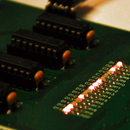
Photographing LED strips was a bit harder than I expected...I could only make the image with HDR enabled. The color you see was actually yellow, composed by red and green LEDs lighting up - it was the fourth schedule point from the LED control menu.
The tea I got from my wife serves both as beverage.and as test equipment - the temperature sensor and the water level sensor went in it before I drank it :).
This can be turned into a great hobbyist home automation kit (one that has nothing to do with fish tanks), lights, garage door, sprinkler heads and home security systems are just a few that come into my mind. I will keep on developing this product though, until it finally turns into something people just know about in communities interested in aquariums.
Tasks that still need to be done
- LEDs on the front panel of the Control Box
- Water level and Temperature regulator
- Many hours of testing
Future ideas for the next prototype
- WiFi based communication (ESP32/LinkIt chipset)
- More GPIO channels
- Larger display
- Ideas are welcome
Step 17: Thank You Note

Thanks for reading this very long instructable, I hope it will ring a bell in many people's heads and provide inspiration for projects that are even better! If you liked what you've read and what you've seen, vote for this instructable in the PCB contest! Thanks!
Cheers!

Grand Prize in the
PCB Contest


