Introduction: Programming Digilent FPGAs Using NI Multisim


Whether you just like to tinker in your shop or you work with them professionally, knowing how to use and program FPGAs is a definite plus for anybody. The problem is that every company that makes FPGAs has their own proprietary software that you have to use in order to program the FPGA board.
Luckily National Instruments has made it possible to program many Digilent FPGA boards without having to leave the familiar and ubiquitous Multisim environment. It takes some work to do the initial set up, but once everything is all set up correctly, you'll be programming FPGAs in no time.
Step 1: Get the Correct Tools
In order to make this work, you will need to have several programs installed and working on your computer.
LabVIEW 2014 or higher (click here for more LabVIEW info and to download from NI)
Multisim 14.0 or higher (click here for more Multisim info and to download from NI)
Install LabVIEW first as some of Multisim's files need LabVIEW to already be installed if you want them to talk to each other. Be sure to restart your computer after each program is finished installing.
Note that when I installed LabVIEW 2016, it installed into "C:\Program Files\National Instruments" and not "C:\Program Files (x86)\National Instruments". Since Multisim and LabVIEW need to talk to each other, I moved the LabVIEW directory into "C:\Program Files (x86)\National Instruments" to ensure that they could. I don't know if this is absolutely necessary as I didn't try it before to find out. Be sure to move LabVIEW 2016 before you try and open it to avoid any possible issues.
You will also need one of Digilent's newer FPGA boards built around the Artix-7 chip.
Be aware that this same process can be applied to Digilent's older FPGA boards built around the Spartan-6 chip, but you'll need to have Xilinx's older ISE environment installed. I'll only focus on Vivado in this I'ble, so I leave it to you to ensure you have the correct ISE specific files.
The rest of the process is outlined in an NI white paper tutorial that may help. I will walk through the same steps, but with more pictures and clarity.
In order to correctly link Multisim with Vivado, you need to install the FPGA tool. Click on NI LabVIEW FPGA Vivado 2014.4 to go to the download page for the tool module.

The recommended "NI Download Manager" option installs a small downloader program that will then download the installer. The "Browser Download" option downloads the installer as a *.iso image file, which will then auto-mount itself in your optical drive. Pick either one. I used the "Browser Download" option without a physical optical drive in my machine and it worked perfectly fine.
If the *.iso file does not auto-mount then double click on it to open it from your default Downloads folder. Double click on Setup.

Click on "Next" and then enter one of the serial numbers that came with your install materials. I used the LabVIEW serial number.

The software will do a quick search for any updates. Accept any that show up then click "Next".

Accept the 3 License Agreements and click "Next".

Click "Next" again to begin installation.

Get some popcorn while you watch the progress bar.

Once the install is complete, be sure to restart your computer.
After restarting, navigate to "C:\NIFPGA\programs\Vivado2014_4\data\xicom\cable_drivers\nt64\digilent" on your hard drive and run the "install_digilent.exe" file. This will install Digilent Adept, if needed. Follow the onscreen prompts to complete the install.

Now that all of the correct programs and associated files are installed, let's get to programming some logic.
Step 2: A Word About "Writing" the "Code" for FPGAs
Code for FPGA chips is written in one of several hardware description languages, with the two most common being VHDL or Verilog. Within most of these HDL languages there are two different schools of thought used to write the code for the project, structural or behavioral. These methods are not language specific, but are instead conceptual methods of thinking of how to write the code. You can even use both methods in the same project if you wish with no issues.
In a behavioral design, you simply tell the compiler what you want to do and it will work it's magic in the background and compile the code in a way that the chip can understand it. Here is an example of a two-bit full adder with carry-in:
// Verilog example of a behavioral design
module Full_Adder_behavioral(
    input A,
    input B,
    input Cin,
    output  S,
    output Cout
    );

    wire [1:0] sum;

    // The next line makes it clear what we have. All three terms are added
    // together, so we must have an adder. We've described the behavior of
    // the circuit. Note the absence of any logic declarations like "AND" or "&".
    assign sum = A + B + Cin;
    assign S = sum[0];
    assign Cout = sum[1];
endmodule
When you add three bits, the largest value you can get is decimal 3, or binary 11, so we need the 'sum' value as a two-bit placeholder for the summed bits. The compiler understands what "+" means and builds a binary adder to perform the task. The S and Cout bits are assigned to the respective bits in 'sum'.
In contrast, structural design is an explicit description of the exact logic required to process the input data correctly. Here is the same full adder, but described structurally:
// Verilog example of a structural design
module Full_Adder_structural(
    input A,
    input B,
    input Cin,
    output S,
    output Cout
    );

    // Here we see the use of several logic gate structures. Without deciphering
    // the logic, it would be difficult at best to know what exactly is going on
    // just by glancing at the code. Now imagine a large project with 100s of
    // lines of code to decipher.
    wire w01 = A ^ B;
    wire w02 = Cin & w01;
    wire w03 = A & B;

    assign S = w01 ^ Cin;
    assign Cout = w02 | w03;

endmodule
In this example, we have explicitly told the compiler exactly how we want the input data to be logically processed. The compiler again works its magic and compiles a file that the chip can understand. Exactly how and what it compiles is beyond the scope of this Instructable, but suffice it to say that both examples will result in pretty much the same netlist and program file.
I told you all of that to tell you this. Since Multisim is a circuit design program that utilizes images, we will be "writing" our code by utilizing the structural design method. But with pictures and not words. What do I mean? Here's the same full adder circuit as before, copied directly from the Multisim canvas, but this time with images of the logic gates used:

We are clearly building a logic circuit, and if visually describing the structure of the circuit isn't a structural method of coding, I don't know what you would consider should qualify. And with Multisim, this is all that is needed to program the board. Let's look at how.
Step 3: Now Let's Write Some Code
Well, more like draw a picture, but you get the idea. Let's start with the full adder circuit from the previous step.
Open Multisim and you should see the default blank canvas for designing and simulating analog circuits.

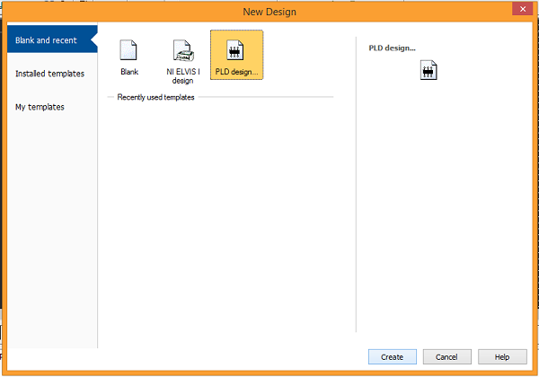
Move up to the top left and click on "File" and select "New".

In the window that pops up, click on the "PLD design" button at the top and then "Create" at the bottom.
The next window lets you pick your configuration file. This is where you can choose the various Digilent board definitions that were loaded during the install process. You can choose a standard definition from the drop menu, you can load a custom configuration file if you have one, or you can create an empty PLD project. For this project I'll be using Digilent's Basys 3 FPGA trainer board. Click "Next" once you have your board selected.

Give your project a name in the next window. Since I'll be building a full adder, that seems appropriate here. Click "Next" once you're done.

In the next window you can select all of the external I/O peripherals attached to the board that you want to add to the project. For this project, I'll need 5 LEDs and 3 switches, so I chose LED0 → LED4 and SW0 → SW2. Click "Finish" after you've made you selections.

The PLD project will now appear in the Design Toolbox on the left side of the Multisim window and the canvas will now display the selected I/O connectors.

There are two ways to place components. The first is to click on the small icon of an AND gate in the tool bar. This will open the component picker window and default to the "PLD Logic" group filter. The second option is to click on "Place" in the menu bar at the top and then select "Component" to open the same component picker window.

For this project we'll be using basic logic gates, so select that from the menu on the left and highlight the first gate you want to place. Place it, then select the next gate. Keep placing gates until you have all that you need. We'll need 2 XOR2, 2 AND2, and 1 OR2 gate for the full adder. Connect everything like in the image below. Note that while you can change the connector labels, it is not recommended.

Step 4: Programming the FPGA
The next step is to send the code to the FPGA. Make sure that your FPGA board is connected via USB and that it is turned on. Then click on "Transfer" in the menu bar and select "Export to PLD..."

In the next window you can select one of several options. Click the radio button to select "Program the connected PLD".

In the next window be sure that the "NI LabVIEW FPGA" tool option is highlighted in the box. Click "Finish" at the bottom to program the FPGA. I also tried using the "Xilinx Vivado 2016.4" option and it worked fine.

Multisim will then connect to Vivado to generate the correct files it needs to program the board. This may take several minutes. Once the 4 steps are complete, your board is programmed and ready.

Here is my Basys 3 with the Full Adder circuit loaded.

Step 5: Some Notes About Configuration Files
Multisim uses configuration files to communicate between Multisim and Vivado. Each board requires two, one with extension *.mspc file and the other with either *.ucf or as *.xdc. If you have either the Basys 3 or the Nexys 4 DDR (not the original Nexys 4) these files are either missing or incomplete, so here is a quick walkthrough on how to add and/or modify them. If you are using any other board, you can skip this step.
For the Nexys 4 DDR the files are not included by default, so first be sure that Multisim is not running. Then download the DigilentNexys4DDR.mspc and DigilentNexys4DDR.xdc files at the bottom of this step. Next, navigate to the Multisim directory where the configuration files are stored. The path name should be something similar to "C:\Program Files (x86)\National Instruments\Circuit Design Suite 14.1\pldconfig". Once there, move the two downloaded files into this folder. Open Multisim and program a project to your Nexys 4 DDR as outlined in the previous steps.
The Basys 3 configuration files that are packaged with Multisim when you install it are missing some definitions. If you simply want to download the correct versions and overwrite the existing files, download the DigilentBasys3.xdc and DigilentBasys3.mspc files at the bottom of this step. Navigate to the Multisim directory as noted above and overwrite the existing two Basys 3 files. If you want to go through the process of modifying the files, continue reading.
When you open a new PLD project in Multisim and select the Basys 3 as your target board, there are several I/O options that are missing. Specifically, the definitions for the VGA, RS-232, USB HID(PS/2), and quad SPI flash are all missing.

In order to fix this, we need to modify these installed configuration files. To find them, first make sure that Multisim is not running, then navigate to the root directory for Multisim. The file path should be similar to "C:\Program Files (x86)\National Instruments\Circuit Design Suite 14.1\pldconfig". Find the two files labeled "DigilentBasys3". One file has a .xdc extension, the other has a .mspc extension.

Before going any further, be sure to make a copy of these two files and place the copies in a separate directory and folder, like a new folder on your desktop. In the event something doesn't work, you can copy the original versions and try again. I also don't recommend you modify the files unless you are confident in your abilities. Erroneous changes won't affect Mutisim's performance, but your board won't program properly.
In order to make the changes, you need to use a text editor like Notepad++. Don't double click the .mspc file to open it. It will open Multisim, which is of no use to you at this point. You need to edit the actual text in the file that Multisim reads to load the correct board configuration, so right click on it and select "Open with..." Select your text editor from the options available. .mspc files are written in a mark-up language format, similar to HTML or XML. It's a simple format but it needs to be correct.

There is no need to modify any of the data in the top section (text lines 1-9 in the image). The portion we are concerned with is all the data between the <pins> tags. Each I/O pin definition requires a few basic parameters to define it. The "Name" should match the pin name that is found in the .xdc file (more on that in a bit). The "Mode" determines whether the pin is defined as an input ("in"), output ("out"), or bidirectional pin ("bidir"). "Location" tells Multisim on which side of the canvas the pin should be placed by default. Inputs are normally on the left, while outputs are normally on the right. The "Place" option is simply a boolean valued flag that tells Multisim whether to have that I/O pin selected by default when you first select your I/O pins. Scroll back up two images and note the check marks in the boxes. These are the pins selected by default.
You are welcome to add the missing pins on your own as needed, or you can copy and paste the definitions found here.
<Pin Name="vgaRed0" Mode="out" Location="left" Place="0"/>
<Pin Name="vgaRed1" Mode="out" Location="left" Place="0"/>
<Pin Name="vgaRed2" Mode="out" Location="left" Place="0"/>
<Pin Name="vgaRed3" Mode="out" Location="left" Place="0"/>
<Pin Name="vgaBlue0" Mode="out" Location="left" Place="0"/>
<Pin Name="vgaBlue1" Mode="out" Location="left" Place="0"/>
<Pin Name="vgaBlue2" Mode="out" Location="left" Place="0"/>
<Pin Name="vgaBlue3" Mode="out" Location="left" Place="0"/>
<Pin Name="vgaGreen0" Mode="out" Location="left" Place="0"/>
<Pin Name="vgaGreen1" Mode="out" Location="left" Place="0"/>
<Pin Name="vgaGreen2" Mode="out" Location="left" Place="0"/>
<Pin Name="vgaGreen3" Mode="out" Location="left" Place="0"/>
<Pin Name="Hsync" Mode="out" Location="left" Place="0"/>
<Pin Name="Vsync" Mode="out" Location="left" Place="0"/>

<Pin Name="RsRx" Mode="in" Location="left" Place="0"/>
<Pin Name="RsTx" Mode="out" Location="left" Place="0"/>

<Pin Name="PS2Clk" Mode="bidir" Location="left" Place="0"/>
<Pin Name="PS2Data" Mode="bidir" Location="left" Place="0"/>

<Pin Name="QspiDB0" Mode="bidir" Location="left" Place="0"/>
<Pin Name="QspiDB1" Mode="bidir" Location="left" Place="0"/>
<Pin Name="QspiDB2" Mode="bidir" Location="left" Place="0"/>
<Pin Name="QspiDB3" Mode="bidir" Location="left" Place="0"/>
<Pin Name="QspiCSn" Mode="out" Location="left" Place="0"/>
Copy and paste this list into the .mspc text file below the "JXA_" definitions.
Save the updated version of the .mspc file and make sure that this is the file in the "pldconfig" folder in the Multisim directory.
Now open the Basys 3 .xdc file in the text editor. Below the "JXA_" definitions, add the following items.
##VGA Connector
set_property PACKAGE_PIN G19 [get_ports {vgaRed0}]
	set_property IOSTANDARD LVCMOS33 [get_ports {vgaRed0}]
set_property PACKAGE_PIN H19 [get_ports {vgaRed1}]
	set_property IOSTANDARD LVCMOS33 [get_ports {vgaRed1}]
set_property PACKAGE_PIN J19 [get_ports {vgaRed2}]
	set_property IOSTANDARD LVCMOS33 [get_ports {vgaRed2}]
set_property PACKAGE_PIN N19 [get_ports {vgaRed3}]
	set_property IOSTANDARD LVCMOS33 [get_ports {vgaRed3}]
set_property PACKAGE_PIN N18 [get_ports {vgaBlue0}]
	set_property IOSTANDARD LVCMOS33 [get_ports {vgaBlue0}]
set_property PACKAGE_PIN L18 [get_ports {vgaBlue1}]
	set_property IOSTANDARD LVCMOS33 [get_ports {vgaBlue1}]
set_property PACKAGE_PIN K18 [get_ports {vgaBlue2}]
	set_property IOSTANDARD LVCMOS33 [get_ports {vgaBlue2}]
set_property PACKAGE_PIN J18 [get_ports {vgaBlue3}]
	set_property IOSTANDARD LVCMOS33 [get_ports {vgaBlue3}]
set_property PACKAGE_PIN J17 [get_ports {vgaGreen0}]
	set_property IOSTANDARD LVCMOS33 [get_ports {vgaGreen0}]
set_property PACKAGE_PIN H17 [get_ports {vgaGreen1}]
	set_property IOSTANDARD LVCMOS33 [get_ports {vgaGreen1}]
set_property PACKAGE_PIN G17 [get_ports {vgaGreen2}]
	set_property IOSTANDARD LVCMOS33 [get_ports {vgaGreen2}]
set_property PACKAGE_PIN D17 [get_ports {vgaGreen3}]
	set_property IOSTANDARD LVCMOS33 [get_ports {vgaGreen3}]
set_property PACKAGE_PIN P19 [get_ports Hsync]
	set_property IOSTANDARD LVCMOS33 [get_ports Hsync]
set_property PACKAGE_PIN R19 [get_ports Vsync]
	set_property IOSTANDARD LVCMOS33 [get_ports Vsync]


##USB-RS232 Interface
set_property PACKAGE_PIN B18 [get_ports RsRx]
	set_property IOSTANDARD LVCMOS33 [get_ports RsRx]
set_property PACKAGE_PIN A18 [get_ports RsTx]
	set_property IOSTANDARD LVCMOS33 [get_ports RsTx]


##USB HID (PS/2)
set_property PACKAGE_PIN C17 [get_ports PS2Clk]
	set_property IOSTANDARD LVCMOS33 [get_ports PS2Clk]
	set_property PULLUP true [get_ports PS2Clk]
set_property PACKAGE_PIN B17 [get_ports PS2Data]
	set_property IOSTANDARD LVCMOS33 [get_ports PS2Data]
	set_property PULLUP true [get_ports PS2Data]


##Quad SPI Flash
set_property PACKAGE_PIN D18 [get_ports {QspiDB0}]
	set_property IOSTANDARD LVCMOS33 [get_ports {QspiDB0}]
set_property PACKAGE_PIN D19 [get_ports {QspiDB1}]
	set_property IOSTANDARD LVCMOS33 [get_ports {QspiDB1}]
set_property PACKAGE_PIN G18 [get_ports {QspiDB2}]
	set_property IOSTANDARD LVCMOS33 [get_ports {QspiDB2}]
set_property PACKAGE_PIN F18 [get_ports {QspiDB3}]
	set_property IOSTANDARD LVCMOS33 [get_ports {QspiDB3}]
set_property PACKAGE_PIN K19 [get_ports QspiCSn]
	set_property IOSTANDARD LVCMOS33 [get_ports QspiCSn]
Save the updated .xdc file and make sure it is in the "pldconfig" folder. Navigate again to the "pldconfig" file and verify that the "Date Modified" tag shows the correct date of modification and not the date you installed Multisim.

Once you have these files modified, it's time to check them and make sure they work. Open Multisim and start a new PLD. You should now see all of the board I/O available for selection during that particular configuration step.

If you have any problems with this process, feel free to post your questions here, but a much better place would be the Digilent forum.

Step 6: That's It!!
As you can see, programming FPGAs is really simple with Multisim. You only need a working knowledge of how logic circuits work. You certainly don't need to go through the struggle of learning a completely new HDL programming language.
As always, thanks for reading. If you have questions, please ask them in the comments below, though PMs are always welcome as well. You just never know when someone else has the same question and that way we can all learn and help each other get better. Have fun building!
Also, please check out the Digilent blog where I contribute from time to time. Just click the image below.