

Introduction: Monitoring Digital Circuits With the Digital Discovery


Monitoring digital circuits can be difficult at best. Sometimes it's nigh impossible. But the Digital Discovery makes it easier to monitor and troubleshoot complex digital circuits.
In this Instructable, I will show how to monitor simple digital signals with a rather not-so-complex digital modulo 10k counter and 7-segment LED display.
The code for the counter itself is written in Verilog and loaded onto a Digilent CMOD A7 bread-board compatible FPGA board. That being said, this is not a Verilog or FPGA tutorial. However the concepts behind the code will hopefully be explained enough so that you can use any other type of programmable chip and whatever language you are familiar with to follow along.
The overall design and source code for this project is not my own but comes from the Verilog edition of Digital Design with some slight modifications to get it to work for this exact project. I will go over each individual logic block used in the design one at a time, and then tie them all together at the end.
Once the code is defined and explained, I'll describe the external driver circuit for the LED display.
Lastly, I'll go over how to use the Digital Discovery to monitor the signals.
For this project you will need:
- Digilent Digital Discovery.

- Digilent Waveforms 2015 software.

This is a free software download and is required to interface with the Digital Discovery.
- Digilent CMOD A7.

The A7 was chosen specifically because it has very few built-in peripheral devices on the board, i.e. no 7-segment LED display. As mentioned, any programmable chip and board will work for this.
- Xilinx Vivado HLx tool suite. This is a free download that is compatible with Xilinx's family of FPGA chips. The A7 version I will be using uses the XC7A35T-1CPG236C chip.
- 7-segment LED display.
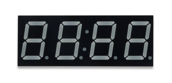
I used a common-cathode MSQ6941C, but a common-anode version will work with some design tweaks.
- 4X NPN BJT transistors.
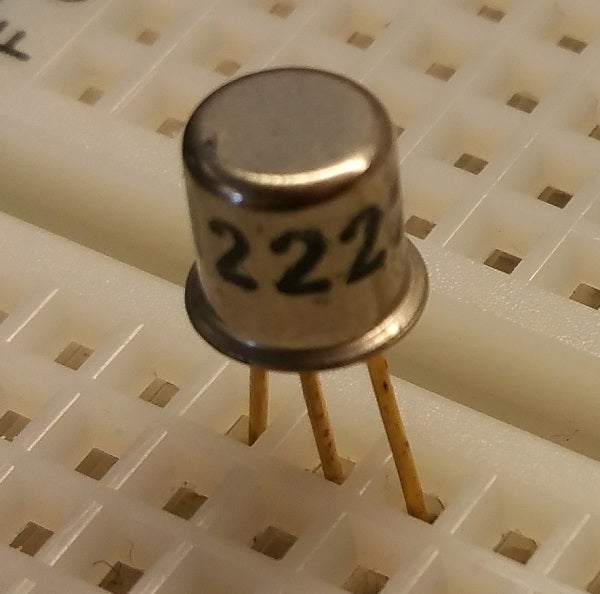
I used 2N2222A, but this project won't be picky with a specific NPN version. These are used to control the cathode signals. The FPGA pins are not meant to drive high power loads, and while an LED might not seem like much, it's good practice to protect your chip FPGA by buffering the signal with a transistor. If you are using a common-anode display you will need to use PNP transistors on the anodes.
- solderless bread-board and wires.
Whatever works to make connections on the bread-board. Depending on your setup, you may need to use a couple of bread-boards.
- 12X resistors.
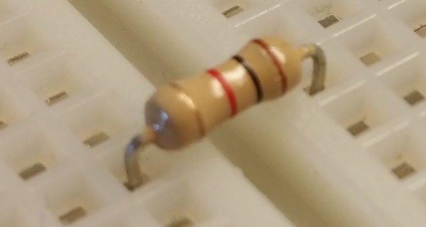
5X 1kΩ resistors, one for each BJT base pin and one for the decimal point pin on the 7-segment display since it won't be used and can be driven low to keep it turned off.

7X 150Ω resistors, one for each segment anode pin on the display.
Step 1: The Clock Divider.
The first block we will define is a clock divider, which is then used to drive the counter block and the 7-segment block. The A7 system clock is 12 MHz, so if we define a minimum 20-bit bus and toggle the LSB with the system clock, we can pick and choose any bit n (n starting at 0) and get a 2n+1 factor of 12 MHz. So if we use the first bit we would get 12 MHz / 20+1 = 6 MHz. The 2nd bit gives us 12 MHz / 21+1 = 3 MHz and so on.
Based on this, we will define 2 additional clocks using this divider. One will be driven from bit 15 to give us a 183 Hz clock and will be used by the 7-segment driver block as the segment refresh rate. You want to have each segment refresh at about 50 Hz, and since we are using 4 segments, we need ≈ 200 Hz to drive the segment refresh rate.
The second clock will be taken from bit 20 and will give us a 5.7 Hz clock which will be used by the counter block to increment the value shown on the display. Using a lower bit value will increase the count rate by some integer multiple of 2, i.e. bit 19 would increment the count at 11.4 Hz.
Here's the code:
module clkdiv(
    input wire mclk,
    input wire clr,
    output wire clk183,
    output wire clk6
    );

    reg [23:0] q;

    always @(posedge mclk or posedge clr)
    	begin
    		if(clr == 1)
    			q <= 0;
    		else
    			q <= q + 1;
    	end

    assign clk183 = q[15];  //183Hz
    assign clk6 = q[20];   //6hz
endmodule
Step 2: The 10k Counter
Next we define the block that will count from 0-9999 and then reset back to 0. This block works much like the clock divider block, but instead of picking off individual bits from the bus, we will export the entire bus.
9999 in decimal = 0010 0111 0000 1111 in binary, so we need to define a 14-bit bus as the output. As long as the "clr" button is not pressed or the count is not 9999, q will increment by 1 for each clock pulse. The clock pulse used is the 5.7 Hz signal defined in the previous step, so the display will increment at that rate.
Here's the code:
module mod10kcount(
    input wire clr,
    input wire clk,
    output reg [13:0] q
    );

    always @(posedge clk or posedge clr)
    	begin
    		if(clr == 1)
    			q <= 0;
    		else if(q == 9999)
    			q <= 0;
    		else
    			q <= q + 1;
    	end
endmodule
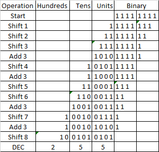
Step 3: The Binary to Binary-Coded-Decimal Converter
The 10k counter block outputs a 14-bit binary value. The problem is that it is in binary, which is simple to use but doesn't convert straight over to decimal without some work.
We can use hexadecimal digits to represent 4 binary digits, where one digit has the ability to accurately reflect the value of 4 binary digits representing the decimal values 0-15. With decimal, one digit can only accurately display up to "9", and then an additional digit is required to display the values 10-15. To do the conversion, we will use the double dabble, or shift-and-add-3, algorithm. I will leave it to you to verify that it works.
The algorithm is as follows for an n-bit binary value:
1) Shift the binary number left one bit.
2) If n shifts have occurred, the BCD number is accurately represented in the Units, Tens, Hundreds, etc. columns.
3) If the binary value in any of the BCD columns is greater than or equal to 5 after shifting, add 3 to that value in that BCD column. (Be sure to check the value and add accordingly for each column separately!)
4) Go to 1).
This is illustrated in the table below starting with the binary value for 255, or 1111 1111.
Here's the code:
module binbcd14(
    input wire [13:0] b,
    output reg [16:0] p
    );

    reg [32:0] z;
    integer i;

    always @(*)
    	begin
    		for(i = 0; i <= 32; i = i + 1)
    			z[i] = 0;
    		z[16:3] = b;

    		repeat(11)
    			begin
    				if(z[17:14] > 4)
    					z[17:14] = z[17:14] + 3;
    				if(z[21:18] > 4)
    					z[21:18] = z[21:18] + 3;
    				if(z[25:22] > 4)
    					z[25:22] = z[25:22] + 3;
    				if(z[29:26] > 4)
    					z[29:26] = z[29:26] + 3;
    				z[32:1] = z[31:0];
    			end
    		p = z[30:14];
    	end
endmodule
Step 4: The 7-segment LED Driver
7-segment displays are pretty common and really easy to use. To display the value "1", we need to have two of the seven segments on and the other five off. This data is easily represented in binary, but requires some conversion from standard binary. Of course.
For a good tutorial on 7-sement displays and how they work, check out the Digilent Learn site. The tutorial at electronics-tutorials.ws is another good option.
The code contains a couple of case statements that determine which value to display and on which digit of the 7-segment display to put it.
A 0-3 counter s takes the 5.7Hz clock as its trigger. The value of s is used to determine which anode is turned on as well as which 4 bits of the 16-bit binary input is used. The binary value of the digit is then converted to the 7-segment binary value that represents that digit.
Normally you would drive the cathode value low and the anode value high in order to turn on the LED. But since we are using NPN BJTs, we need both cathode and anode values to be driven high in order to turn on the LED.
Here's the code:
module x7segbc(
    input wire [15:0] x,
    input wire cclk,
    input wire clr,
    output reg [6:0] a_to_g,
    output reg [3:0] cath
    );

    reg [1:0] s;
    reg [3:0] digit;
    wire [3:0] cen;

    assign cen[3] = x[15] | x[14] | x[13] | x[12];
    assign cen[2] = x[15] | x[14] | x[13] | x[12] | x[11] | x[10] | x[9] | x[8];
    assign cen[1] = x[15] | x[14] | x[13] | x[12] | x[11] | x[10] | x[9] | x[8] | x[7] | x[6] | x[5] | x[4];
    assign cen[0] = 1;

    always @(*)
    	case(s)
    		0: digit = x[3:0];
    		1: digit = x[7:4];
    		2: digit = x[11:8];
    		3: digit = x[15:12];
    		default: digit = 4'b0000;
    	endcase

    always @ (*)
		case (digit) //gfedcba '1' = seg_on
		  	0: a_to_g = 7'b0111111;
		  	1: a_to_g = 7'b0000110;
		  	2: a_to_g = 7'b1011011;
		  	3: a_to_g = 7'b1001111;
		  	4: a_to_g = 7'b1100110;
			5: a_to_g = 7'b1101101;
			6: a_to_g = 7'b1111101;
		  	7: a_to_g = 7'b0000111;
		  	8: a_to_g = 7'b1111111;
		  	9: a_to_g = 7'b1101111;
		  	'hA: a_to_g = 7'b1110111;
		  	'hb: a_to_g = 7'b1111100;
		  	'hC: a_to_g = 7'b1011000;
		  	'hd: a_to_g = 7'b1011110;
		  	'hE: a_to_g = 7'b1111001;
		  	'hF: a_to_g = 7'b1110001;
		endcase

	always @(*)
		begin
			cath = 4'b0000;
			if(cen[s] == 1)
				an[s] = 1;
		end

	always @(posedge cclk or posedge clr)
		begin
			if(clr == 1)
				s <= 0;
			else
				s <= s + 1;
		end

endmodule
Step 5: The Top Control Block
Once you have each logic block defined, you can tie them all together in a top module. The connections between the external pins on the board and the internal logic blocks are defined here, as well as some internal wires to connect the blocks to each other as needed. There are also 3 led0_X assignments that turn off the on-board RGB led built onto the A7. The 3 colors will be set at about 50% brightness by default because the pins will float if you don't drive those pins high in code. Unless you decide to use them, then do what you want.
Here's the code:
module mod10kcount_top(
    input wire sysclk,
    input wire btn,
    output wire [6:0] seg,
    output wire [3:0] cath,
    output wire led0_r,
    output wire led0_g,
    output wire led0_b
    );

    wire [16:0] p;
    wire clr, clk6, clk183;
    wire [13:0] b;

    assign clr = btn;
    assign led0_b = 1;
    assign led0_g = 1;
    assign led0_r = 1;

    clkdiv U1 (
    	.mclk(sysclk),
    	.clr(clr),
    	.clk183(clk183),
    	.clk6(clk6)
    );

    mod10kcount U2 (
    	.clr(clr),
    	.clk(clk6),
    	.q(b)
    );

    binbcd14 U3 (
    	.b(b),
    	.p(p)
    );

    x7segbc U4 (
    	.x(p[15:0]),
    	.cclk(clk183),
    	.clr(clr),
    	.a_to_g(seg),
    	.cath(cath[3:0])
    	);

endmodule
Below are the constraint file definitions I used for the A7 board.
# Clock signal 12 MHz
set_property -dict { PACKAGE_PIN L17   IOSTANDARD LVCMOS33 } [get_ports { sysclk }]; #IO_L12P_T1_MRCC_14 Sch=gclk
create_clock -add -name sys_clk_pin -period 83.33 -waveform {0 41.66} [get_ports {sysclk}];

# LEDs
set_property -dict { PACKAGE_PIN B17   IOSTANDARD LVCMOS33 } [get_ports { led0_b }]; #IO_L14N_T2_SRCC_16 Sch=led0_b
set_property -dict { PACKAGE_PIN B16   IOSTANDARD LVCMOS33 } [get_ports { led0_g }]; #IO_L13N_T2_MRCC_16 Sch=led0_g
set_property -dict { PACKAGE_PIN C17   IOSTANDARD LVCMOS33 } [get_ports { led0_r }]; #IO_L14P_T2_SRCC_16 Sch=led0_r

# Buttons
set_property -dict { PACKAGE_PIN A18   IOSTANDARD LVCMOS33 } [get_ports { btn }]; #IO_L19N_T3_VREF_16 Sch=btn[0]

# 7-seg
set_property -dict { PACKAGE_PIN U4    IOSTANDARD LVCMOS33 } [get_ports { cath[3] }]; #IO_L11P_T1_SRCC_34 Sch=pio[38]
set_property -dict { PACKAGE_PIN V5    IOSTANDARD LVCMOS33 } [get_ports { cath[2] }]; #IO_L16N_T2_34 Sch=pio[39]
set_property -dict { PACKAGE_PIN W4    IOSTANDARD LVCMOS33 } [get_ports { cath[1] }]; #IO_L12N_T1_MRCC_34 Sch=pio[40]
set_property -dict { PACKAGE_PIN U5    IOSTANDARD LVCMOS33 } [get_ports { cath[0] }]; #IO_L16P_T2_34 Sch=pio[41]

set_property -dict { PACKAGE_PIN U2    IOSTANDARD LVCMOS33 } [get_ports { seg[0] }]; #IO_L9N_T1_DQS_34 Sch=pio[42]
set_property -dict { PACKAGE_PIN W6    IOSTANDARD LVCMOS33 } [get_ports { seg[1] }]; #IO_L13N_T2_MRCC_34 Sch=pio[43]
set_property -dict { PACKAGE_PIN U3    IOSTANDARD LVCMOS33 } [get_ports { seg[2] }]; #IO_L9P_T1_DQS_34 Sch=pio[44]
set_property -dict { PACKAGE_PIN U7    IOSTANDARD LVCMOS33 } [get_ports { seg[3] }]; #IO_L19P_T3_34 Sch=pio[45]
set_property -dict { PACKAGE_PIN W7    IOSTANDARD LVCMOS33 } [get_ports { seg[4] }]; #IO_L13P_T2_MRCC_34 Sch=pio[46]
set_property -dict { PACKAGE_PIN U8    IOSTANDARD LVCMOS33 } [get_ports { seg[5] }]; #IO_L14P_T2_SRCC_34 Sch=pio[47]
set_property -dict { PACKAGE_PIN V8    IOSTANDARD LVCMOS33 } [get_ports { seg[6] }]; #IO_L14N_T2_SRCC_34 Sch=pio[48]
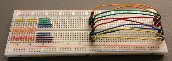
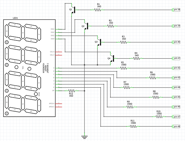
Step 6: The External Display Driver Circuit
The analog circuit used to drive the display is really simple, but there is one thing that could make it slightly confusing. For LEDs to work the cathode must be more negative than the anode, so we should be sending a "0" signal to the cathode pins and a "1" signal to the anode pins. But the BJTs are in between what we have designated as the cathode pins in code on the A7 and the actual LED display cathode pins. NPN BJTs require a positive signal on the base pin in order to turn on, so the code requires a "1" to be output for both cathode and anode pins in order to turn on the LED. The BJT acts kind of like a... buffering inverter here I guess. When it receives a positive signal at the base, the connection across the collector and emitter pins is closed, connecting the LED cathode pin to "0" or GND.
Anyway, here's the best schematic I could make. The LED display shown isn't a perfect match, but no schematic design program has every part ever made. The idea should be clear enough though. On the right are the labels for the pins that match the A7 board.
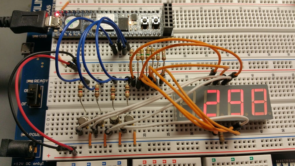
Here's the circuit all put together.
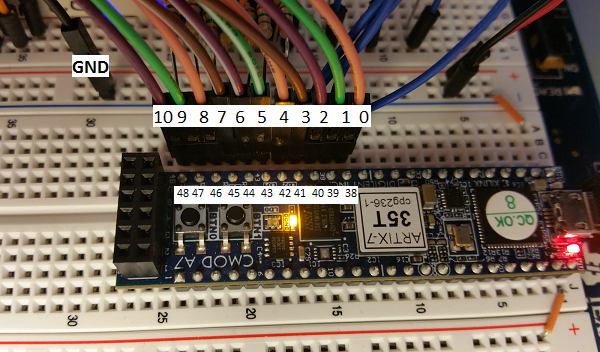
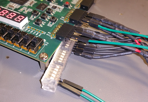
Step 7: Connecting the Digital Discovery
There are additional connection options for the Digital Discovery the Analog Discovery does not have, specifically the two PMOD compatible connectors on either side of the main body.
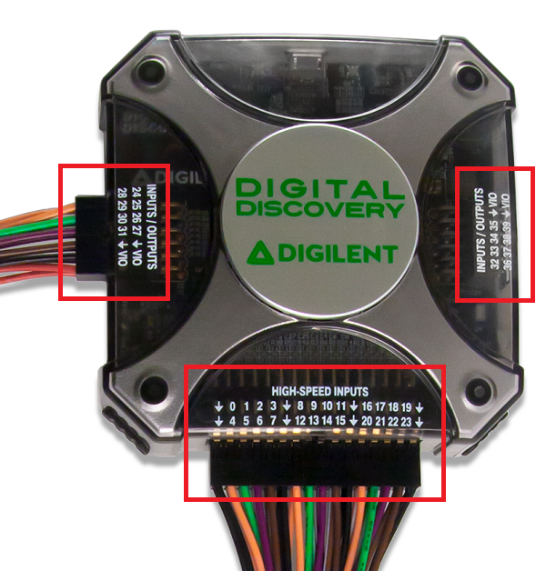
For this project I'm going to stick with the main 32-pin connector and utilize pins 0-10. Pins 0-3 will monitor the 4 cathode signals while pins 4-10 will monitor the 7 anode signals. Simply plug the fly-wires into the bread-board to make the connections. Be sure to connect one of the many GND pins (↓ symbol on the body) on the Discovery to the circuit GND as well. Below I've labeled the A7 pins as well as the Discovery pins to prevent any confusion.
Step 8: Monitoring the Signals. Finally
I'll be using the Logic Analyzer tool in Waveforms for this step. (Go here for a more in depth look at the Logic Analyzer tool and here for a collection of tutorials for all of the Waveforms tool available.)
Let's break up the 11 signals we want to observe into two distinct groups, "digits" and "segments", and then define each group as a bus in the tool window.
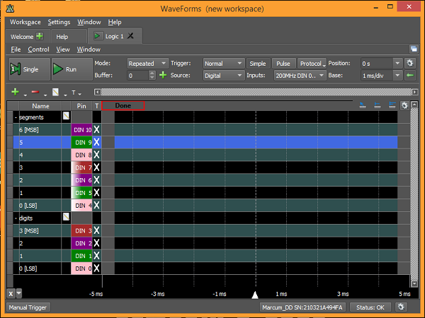
Segment A on the 7-segment display maps to bit 0 of the "segments" bus, with segment G mapping to bit 6. Digit 1 (leftmost) on the display maps to bit 0 of the "digits" bus, with digit 4 mapping to bit 3.
We can observe the data live simply by clicking on the run button at the top. You can adjust the time base of the window to view more or less data in the window. Below you see a full minute of captured date in one window. At about -21 s the count goes from 999 to 1000 so you see the signal for digit 1 turn on. At +6 s I reset the counter. You can see the digits begin to turn on as they are added to the display as the count increments the tens (≈+7.5 s) and then hundreds (≈+23 s) places.
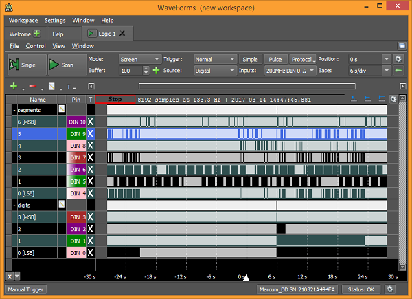
The problem is that if I want to zoom in on this data we start to lose data integrity and it becomes harder and harder to correctly interpret.
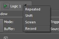
Let's record the data instead. This way we can zoom in or out and not worry about losing data clarity. Click on the button that says "Screen" in the "Mode:" box and select "Record".
The "Single" button will change to "Config". Click on it to configure the record options.
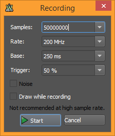
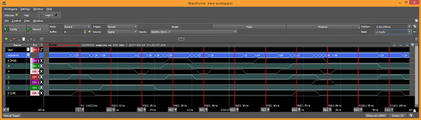
"Samples" lets you determine how many samples will be taken. The rate at which those samples are taken is set in the "Rate" box. The "Base" box lets you determine how long you will be able to record information. You can only set two of the three options, while the software will do its best to auto-set the third value based on your other two choices. Since this project is running pretty slow, let's go with 6,000,000 samples at 10 kHz. The Base box should auto-fill with 1 min. Click "Start" once you have the configuration set. You should see something like this:
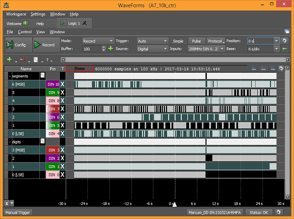
At about +8 s I reset the counter, so you can see all of the digits reset, then digit 4 is on while the count is 0-9, then digit 3 turns at about +10 s and digit 2 turns on at about +26 s.
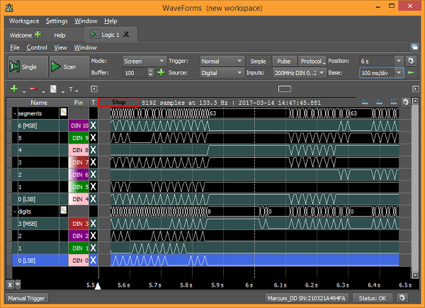
Since I recorded the data, when I zoom in you can clearly see the rising/falling edges of the data.
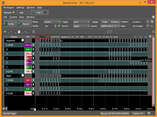
In this image we can see the time it took for the FPGA chip to reset, retrieve the saved program file from flash memory, load it, and start counting again. The digit signal starts again and then very soon after the data for the segments starts up. If we zoom in even more we can start to pick out the actual data. Let's look at the data at +8.17 s, right before I reset the counter.
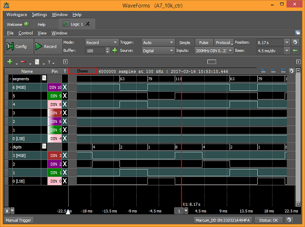
You can see that in the "digits" bus, bit 3 is high, so digit 4 (the rightmost digit) is high, and therefore that digit is turned on. Moving up into the "segments" bus and starting with bit 0 (segment A) we can see that bits 0, 1, 2, 3, 5, and 6 are all high while bit 4 is low. So segments A, B, C, D, F, and G are all on while segment E is off. This pattern corresponds to the pattern for the decimal digit "9" and is displayed in the Ones place.
Moving right to about +6 ms, we see that digits[2] is on, and segments[0, 1, 2, 3, 5, 6] are all high. This matches the previous pattern so we should also see a decimal "9" on the display in the Tens place.
Moving right again to about +11 ms, digits[1] is on and segments[0, 1, 2, 3, 4, 5] are all high. This pattern is for the decimal digit "0", so we should see "0" in the Hundreds place.
Lastly, at about +18 ms digits[0] is high and segments[0, 1, 2, 3, 6] are all high. This pattern corresponds to the decimal digit "3" and is displayed in the Thousands place.
We can therefore conclude that the value of the counter when I reset it was 3099.
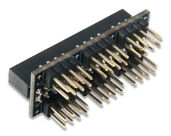
At this point we're done with this project. By default the Digital Discovery can sample up to 200 million samples per second. The next step goes over how to use the High-Speed Adapter for the Digital Discovery to monitor signals at up to 800 million samples per second.
Step 9: Using the High Speed Adapter
The Logic Analyzer tool for the Digital Discovery has a sample rate of 200 MS/s. By adding the High Speed Adapter and using the included high-speed logic probes, we can increase the sample rate up to 800 MS/s. To do this, select the "800MHz DIN 0..7" option in the "Inputs" box above the acquisition window. The Digital Discovery will re-allocate the resources used to sample channels 8-23, limiting us to using channels 0-7.

Since the speed of the CMOD A7 clock is only 12 MHz, I'm going to substitute in the Nexys 4 for this step, which has a core clock of 100 MHz. I really want to try and push the capabilities of the Digital Discovery. The program blocks are all the same but the code is adapted to be used on the Nexys 4. The Vivado project file is included as a zipped file.
Using the 100 MHz clock to drive the 10k counter means that the 7-segment will be counting so fast that you'll never see the digits change. But if, in the program code, we tie the segment signals and one of the anode signals to several of the pins tied to the PMOD connectors JA and JB, we can use the HSA to observe these signals.
Each high-speed probe comes as a twisted pair, one red and one black wire.

When looking at the HSA, the topmost and bottommost rows of pins are all tied to GND (blue boxes) while the two innermost rows of pins correspond to pins 0-23 (red boxes).
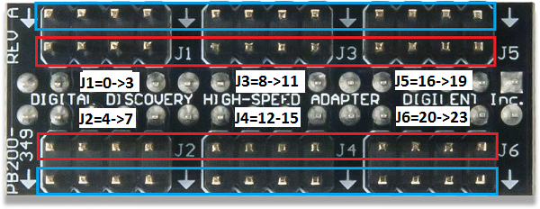
Simply connect the high-speed probes so that the black wire connects to GND and the red wire connects to the associated input port.
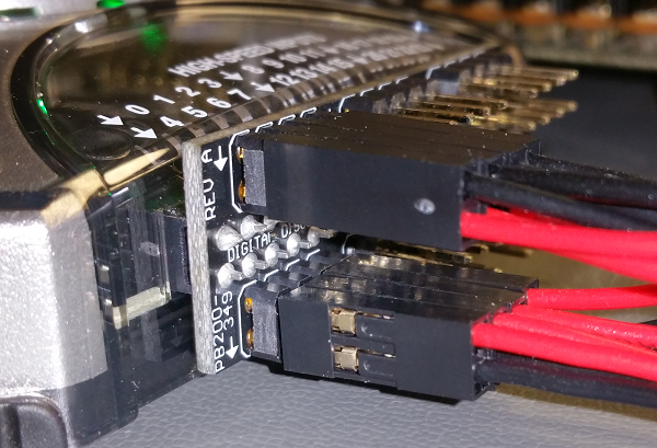
Now here's the tricky part. All of the black GND wires are tied to the Nexys PMOD GND pins through a couple of jumper wires using a small bread-board power strip. The red wires are tied to the several pins on the PMOD connectors JA and JB. The heat shrink tubing on the probes won't allow for more than three probe wires to be placed next to each other on the PMOD header, so you have to get a little creative. Luckily there are a lot of pins to work with on the Nexys.
Once we have all of the connections made we can get to collecting the data. We will need to use the record option again, so configure the settings as follows:

Click on "Start" and you should get something like the following. Click here for a much clearer, higher resolution version.

I added some cursors to highlight some timing blocks. You can see clear differences between the blocks when you look at the "segments" bus. If you look close at the "digit" signal at the top, you'll see that in the first block I have highlitghted it goes low. I have the anode signal to digit 4 (rightmost) connected here, and during this block we see that digit 4 is turned on. There are three more blocks where the other three digits have their chance to shine, but since I'm limited to only 8 signals if I want to utilize the full 800 MS/s rate, I could only pick one digit.
By zooming in on the data right near the first cursor, we can really start to see what's going on. (high res)

Looking at the "segments" line in the table you'll see a decimal value displayed which corresponds to the binary data shown below in the individual "segments" channels. Taking a look at the decimal value "2" we see that with 7 bits the binary value is "0000010". Remembering that for the Nexys-based code a "0" means that the segment is on, and then mapping the segments as "GFEDCBA", we see that only segment "B" is off. This is a decimal-valued "6".
Looking at the next few decimal values we find that "120" displays a "7", "0" displays an "8", "16" displays a "9", "64" displays a "0", etc. We are cycling through all of the decimal values 0-9 in order and then starting over. Sounds like a clock. It's hard to tell in this view, but by adding a couple more cursors we can measure the distance between two instances of the same value and find that the time is 100 μs. This equates to 10 kHz, which is what we should be expecting for the Thousands place digit using a 100 MHz clock to drive the Ones place digit. When we consider that the Ones place digit is ticking at 100 MHz, then divide that value down by 10 kHz for the Thousands place digit to cycle 0-9, we see that the Thousands place digit is cycling 0-9 at 10 kHz.
Now let's look at the data in the One's place. (high res)
Take a second to look at the high resolution version. I added the cursors to make the data easier to read. From cursor 1 on the left to cursor 11 on the right is a spread of only 100 ns. At 800 MS/s, that comes out to only 800 samples in that time frame. So it looks like we succeeded in pushing the Digital Discovery's capabilities. But let's analyze what we see.
The cursors I added are each separated by 10 ns. If we look at the decimal value displayed in the "segments" line where each cursor is placed, we see that the same pattern of 10 decimal values that we saw when we looked at the Thousands place is displayed, albeit with some added "bonus data". We get some noise in the signal when we have several channels change state all at once. Look between cursors 8 and 9. To change from "121" (binary "1111001") to "36" (binary "0100100") we need 5 values to change state. Each channel changes, but not all at the exact same time. If we look at all of the data, we'll see that the only "bonus data" we get is when the channels are changing states. But note that the correct data is present at the correct time and that there is no errant data on the channels, they just don't all change state at the exact same moment. This is due to propagation delays inherent to the trace routing on the Nexys 4 PCB itself. Some traces are slightly longer than others so the signal takes just a bit longer to get to the end. We don't often think about this because the projects we work on don't often deal with this time scale.
Attachments

Step 10: That's It!
The Digital Discovery is a superb tool that allows you to observe and record high-speed data. By simply dedicating more of the FPGA chip's resources to focus on digital-only applications, a whole world of possibilities opens up.
As always, thanks for reading. If you have questions, please ask them in the comments below, though PMs are always welcome as well. You just never know when someone else has the same question and that way we can all learn and help each other get better. Have fun building!
Also, please check out the Digilent blog where I contribute from time to time. Just click the image below.


