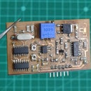
Introduction: Analog SPWM Card for Inverters
Hello everyone and welcome to this amazing article on how I made a SPWM driver card that is capable of generating precisely controlled signals which can be used as input to drive an H-bridge to produce a pure sine wave at the output. This SPWM card purely analog in nature and uses no ASIC ( Application Specific Integrated Circuit ) or microcontrollers. It is completely based out of discrete analog and digital ICs which are either comparators, counters or other ICs. All this is precisely controlled by a crystal to give us accurate frequency output which is 50Hz in this case. Accurate frequency is important here and since we are not using RC based timing components, frequency drift is also minimal.
This project has been a great learning experience for me as an electronics hobbyist. So without further adieu, let's get started!
Step 1: Introduction to the Types of Inverters
Pulse transformer-based
inverter can be widely categorized into two main types depending upon the type of waveform they produce at the output. They are:
- Modified Square wave inverter
- Pure sine wave inverter
Modified Square Wave or Quasi Square wave inverters are the ones where the output waveform is not the traditional sine wave but instead it is a modified version of a pure square wave output with a significant amount of dead-time between the two pulses as seen in the figure above. The output is more like a square wave with an additional step. These inverters are better than pure square wave inverters in terms of reducing harmonics but are not that efficient compared to pure sine inverters.
Modified square wave inverters can actually work reasonably well when driving pure resistive loads but suffer greatly in efficiency and performance when used with inductive and capacitive loads due to the steep rising and falling edge causing a lot of harmonics and heating loss. Most cheap inverters are of Modified Square Wave type.
Pure Sine Wave inverters on the other hand are the more efficient type of inverters because their output is same or nearly as same as that of our mains supply. Since all appliances are designed to run properly with sine wave AC, these inverters are more efficient with least amount of harmonic and heat loss. These inverters are expensive because the involve a lot of complicated switching control, feedback and filtering to produce the desired sine wave output which ideally should not distort with different load types. Sine wave inverters should be a preference while trying to design a renewable energy system.
Step 2: Introduction to SPWM Wave
SPWM stands for Sinusoidal Pulse Width Modulation. It is a type of signal which is essentially square in nature but the duty cycle of the square wave varies in proportion to the amplitude of the square wave. The entirety of the SPWM signal will correspond to the sine wave in terms of time period. So essentially for SPWM, the change in duty cycle is corresponding to the change in amplitude over a given fixed period of time.
A question now naturally arises, how do we generate SPWM signals?
Well to do this we would firstly require the original sine wave signal and then a carrier signal. The idea here is to compare the sine wave signal to a high frequency carrier signal in an almost point to point manner to generate the square wave representation of the given sine wave. The diagram describes the theory
Step 3: Introduction to H Bridge Topoplogy
The figure explains how the basic H bridge works. Here it is seen that a given load is controlled by a total of 4 switches (MOSFETs or BJTs as applicable). At a time two switches have to be activated to either allow current to pass through one direction or the opposite direction. It is also worthy to note that a few combinations are never allowed to happen as they will cause a direct short between the power supply.
Step 4: Using SPWM Signal to Control H Bridge
Having the basic understanding of how SPWM signals look like, how they are generated and how H-bridge works, these concepts can now be integrated together, where SPWM signals can drive the H bridge.
As seen earlier, only a selected combination of MOSFETs are allowed to operate to either allow current flow in one direction or the other direction. For properly activating the H-bridge, we need a total of 4 signals, each of which controls one MOSFET. A pair of MOSFETs are activated every half cycle of the entire wave. The waveforms required are colour coded into blue and red in the attached diagram for a better understanding.
- A pair of SPWM signal and the square wave marked in RED are active at the same time and are used to drive the diagonal pair of MOSFETs for one-half cycle
- The other pair of SPWM signal and the square wave marked in BLUE are active at the same time and are used to drive the other diagonal pair of MOSFETs for the other half cycle
The table attached also shows the combination which can be used to actively switch the H-bridge to get AC signal as output. It also mentions the combination which should NOT be used or it can destroy the complete setup.
Step 5: Why the Analog Approach?
Well, if dedicated SPWM driver cards like the ESG002 are available then why take the hassle of building it out of discrete components which may not be as good as it’s commercial counterparts?
A few reasons:
- While it is a fact that the practicality of such analog SPWM cards are not much, it has been a great project to understand the working of modern-day inverters and power electronics.
- We can get the detailed idea of how discrete digital and analog components like Counters, Timers, Comparators, BJT, crystal oscillators, analog switches etc work and how can we combine them in such a way so as to create meaningful output
Step 6: Block Diagram of the Analog SPWM Card
The image is the block diagram of the entire project and can be broadly classified into the below mentioned sections
- Generation of stable carrier frequency and 50 Hz signal from crystal oscillator
- Filtering of signals to produce triangular waves and clamping
- Point to point comparison using operational amplifiers
- Wave shaping and adjusting of the raw SPWM and square wave signals
- Adding a buffer stage so that finals signals are not distorted by any loading effect.
Step 7: Generation of 50Hz and 16khz Signals
The first and probably one of the crucial parts of this entire project is the generation of stable frequencies. For this a 4.096 Mhz crystal is selected. This crystal will act as a clock source to a binary counter/ divider that will divide the frequency into our desirable range of carrier frequency.
The IC 4060 is a 14-stage binary counter/oscillator IC that can be used to create stable time delays and divide frequencies into several stages. For our application, the incoming 4.096 MHz signal is divided such that we get 16 Khz, that will act as our carrier frequency and also 500Hz, that will later be divided to get our desired 50 Hz
The IC 7490 is a decade and binary counter capable of divide by 5 and divide by 2 functions and can in total divide a frequency by 10 with the correct combination. This divide by 10 can then be used to create 50 Hz from the 500 Hz obtained from the IC 4060.
I have made a separate tutorial on how to generate accurate 50Hz signal. The project details are available on my website as well as instructables
Step 8: Producing Triangular Waves
After successfully obtaining stable 50Hz signal and carrier frequency of 16 Khz, both of these square waves are converted to triangular wave using low pass filter circuits. They are then converted to triangular waves of comparable amplitudes using active clamping circuits. This is useful for the next stage of point-to-point comparison.
Step 9: Regenerating Complimentary Square Waves
After successfully generating the triangular waves, they need to be compared to generate the required SPWM waves as discussed in the theory earlier.
Also it is worth to note that we require 4 signals to drive the H-bridge 2 of which are SPWM signals and 2 of them are square wave signals. It is not possible to use the initial square waves because of the phase shift during generation of the triangular wave. So the 50 Hz triangular wave again needs to be converter to square wave.
Step 10: Getting the SPWM Signals
We now have the required 2 square wave signals, all that is left if to produce the 2 complimentary SPWM signals. With some wave shaping circuit and level shifting, we are able to generate the 2 complimentary SPWM signals by comparing the two triangular waves that we had generated earlier. The raw waveform looks like the image attached
Step 11: Wave Shaping Concept
It is evident from the above pictures that while it is definitely possible to generate SPWM signals but the shape and duration of these signals are not satisfactory. To resolve this we need to again apply some wave-shaping methods and generate a clean looking SPWM wave.
Wave shaping along with signal envelope will give us the desired result.
For wave shaping there are a few stages involving the adjustment of triangular wave amplitudes and adjusting the duty cycle of the square waves. This is done by adjusting voltage levels through potentiometer that control the OP-AMP stages of the wave shaping section.
The images now represent the proper SPWM signals and their comparison to the corresponding square wave
Step 12: Adding a Buffer Stage
A buffer stage at the output is important because after wave shaping section, there are still some portion of the wave which may not be considered an ideal signal to be given to the MOSFET driver.
A good signal to a MOSFET driver should be a square wave with flat top and bottom. Also, the raw signal may be prone to loading effects that can degrade the signal quality and may not trigger the MOSFET driver properly. For this a buffer stage is important which help to keep the shape of the wave intact and reduced loading effect.
Step 13: Final Outputs
With the buffer stage output, we have now acquired all the 4 signals required that can be used to drive the H bridge to produce the AC wave form .
Two complimentary SPWM signals and 2 complimentary 50Hz square wave signals are successfully generated from just a crystal and some creative analog circuitry.
Step 14: Final H Bridge Output
After getting the AC representation of SPWM, this signal can now be passed through a LC low pass filter which can filter out all the high frequency switching and give us with the neat sine wave we were looking for.
Success!
Though it cannot be called a perfect sine wave, minor adjustments can be made by adjusting the potentiometers and bringing the shape closer to sinusoidal one.
Step 15: Conclusion and Final Words
We have successfully generated the required SPWM signals that can be used to actually drive a H-Bridge using pure analog components with stable frequency outputs.
Is this the perfect solution? No, the reason being simple. Microcontrollers and ASIC based cards are specifically designed for this which packs in more precision and much more useful features.
Does this analog card even work? YES !
I have successfully used the signals generated by this card to drive an H-bridge and with proper filtering I was able to get a fairly decent sinusoidal signal.
As an electronics enthusiast this project has been a great learning curve specially in knowing the nitty gritty bits of analog electronics and has given me insights and better understanding of several concepts that can be useful in other projects and applications as well.
I have attached a few snaps of the initial testing of this concept on breadboard.
I have documented this entire project in more detail on my website : www.utsavrshah.in
Over there you can find more detailed snippets and a PDF version of this project for you to refer.
A big thank you to my friend Sayantan Maiti for helping me out solving some of the crucial roadblocks on this project. You can visit his Instructable page here:
https://www.instructables.com/member/SayantanM4/
I hope this project inspires you to create something unique as well. Till then, see you in the next one!


