Introduction: PCB Business Card With NFC
Arriving at the end of my studies, I recently had to look for a six-month internship in the field of electronics engineering. To make an impression and maximize my chances of being recruited in the company of my dreams, I had the idea to make my own business card. I wanted to make something unique, useful and able to demonstrate my electronic circuit design skills to whom I will hand it.
Three years ago, while browsing Instructables, I found a very interesting project made by Joep1986, entitled "Digital Business Card With NFC". This project involved embedding an NFC tag in a paper business card to share contact information with a phone equipped with NFC technology. I found this project very inspiring and I thought replacing the generic NFC tag with a custom circuit of my invention.
This is how I came up with the idea of creating my own business card on a printed circuit board, capable of sending in an instant my LinkedIn profile on a recruiter's smartphone using NFC technology.
This Instructable covers every step I followed to imagine, design and create my PCB business card with NFC, from the antenna parameter calculations to the NFC chip programming through the textured PCB design.
Step 1: BOM, Tools and Skills Needed
You will need:
Necessary tools:
- soldering iron
- hot air rework tool
- solder paste
- solder flux
- solder wire
- long nose tweezers
- cross-lock tweezers
- isopropyl alcohol
- a Q-tip
- a toothpick
- a phone with NFC
Optional (but handy) tools:
- Fume extractor
- Magnificent glass
Skills:
- SMD soldering skills
Bill of materials:
| Component | Package | Reference | Quantity | Supplier |
|---|---|---|---|---|
| NFC chip 1kb | XQFN-8 | NT3H1101W0FHKH | 1 | |
| Yellow LED | 0805 | APT2012SYCK/J3-PRV | 1 | |
| 47 Ω resistor | 0603 | CRCW060347R0FKEAC | 1 | |
| 220 nF capacitor | 0603 | GRM188R70J224KA88D | 1 | |
| PCB | - | - | 1 |
Step 2: The NFC Technology
What is NFC ?
NFC is an acronym for Near Field Communication. It is a short-range radio technology that enables communication between devices that are held in close proximity (< 10 cm). NFC systems are based on traditional High Frequency (HF) RFID, operating at 13,56 MHz.
Currently, the NFC standard supports different data transmission rates up to 424 kbit/s. The principle mechanism of NFC communication between two devices is the same as traditional 13,56 MHz RFID, where there is both a master and a slave. The master is called the emitter, or reader/writer and the slave is a tag or a card.
How does it work ?
NFC always involves an initiator and a target: the initiator (Emitter) actively generates an RF field that can power a passive target (Tag) using electromagnetic induction between two loop antennas:

The antennas of the emitter and the tag are coupled via an electromagnetic field and this system can best be viewed as an air-core transformer where the reader acts as the primary winding and the tag as the secondary winding: the alternating current passing through the primary coil (Emitter) induces a field in the air, inducing current in the secondary coil (Tag). The tag may use the current from the field to power itself : in this case, no battery is required to access it, neither in read nor in write mode. The NFC tag chip draws all needed power to operate from the magnetic field generated by the reader through its loop antenna.
Where is NFC used ?
NFC is a growing technology with the need to wirelessly connect electronic devices. NFC has been widely integrated in smartphones in order to interact with NFC compatible physical devices and provide new services like contactless payment.
Since NFC tags do not need to integrate a power source because they can be powered by the energy emitted by the reader, they can take very simple form factors such as unpowered tags, stickers, cards or even rings.
I really liked the fact that the NFC tags do not embed polluting button cells to operate but use only the transmitter's energy instead.
Step 3: The NFC Chip
NFC IC
The NFC chip is the heart of the business card.
My requirement were:
- a small SMD package
- enough memory for a link to my LinkedIn profile
- embedded energy harvesting module
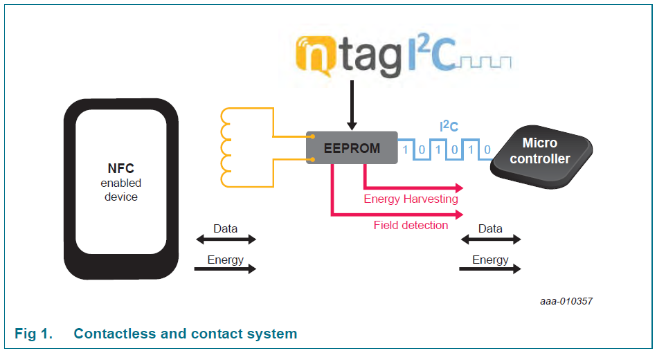
After comparing several NFC modules, I opted for the NTAG NT3H1101 IC from NXP. According to its datasheet:
"The NTAG I2C is the first product of NXP’s NTAG family offering both contactless and contact interfaces (see Figure 1). In addition to the passive NFC Forum compliant contactless interface, the IC features an I2C contact interface, which can communicate with a microcontroller if the NTAG I2C is powered from an external power supply. An additional externally powered SRAM mapped into the memory allows a fast data transfer between the RF and I2C interfaces and vice versa, without the write cycle limitations of the EEPROM memory. The NTAG I2C product features a configurable field detection pin, which provides a trigger to an external device depending on the activities at the RF interface. The NTAG I2C product can also supply power to external (low power) devices (e.g. a microcontroller) via the embedded energy harvesting circuitry."
Attachments
Step 4: Calculating the Antenna Inductance
To communicate and be powered, an NFC tag must have an antenna. The antenna design procedure starts with the equivalent model of the NFC chip and its loop antenna:
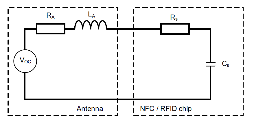
where:
- Voc is the open circuit voltage induced by the magnetic field in the loop antenna
- Ra is the equivalent resistance of the loop antenna
- La is the equivalent inductance of the loop antenna
- Rs is the serial equivalent resistance of the NFC chip
- Cs is the serial equivalent tuning capacitance of the NFC chip
The antenna can be described by an inductor La with a very small loss resistor Ra. When a magnetic field is induced by the emmiter in the loop antenna, a current is induced in it and an open circuit voltage Voc appears at its terminals. The NFC chip can be described by an input resistor Rs and an in-built tuning capacitor Cs.
The series resistors Ra and Rs are summed for the last equivalent model of the circuit consisting of the NFC integrated circuit and its loop antenna:
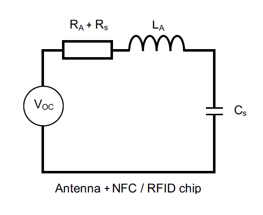
The NFC IC resistor Rs together with the antenna resistor Ra and the in-built capacitor Cs forms a resonant circuit RLC with the inductor La of the antenna. More informations about RLC resonance circuits are explained in online electronics tutorials.
The resonant frequency of a series RLC circuit is given by the formula:

where:
- f is the resonant frequency (Hz)
- L is the equivalent inductance of the circuit (H)
- C is the equivalent capacitance of the circuit (F)
The only unknown parameter of the equation is the value of the inductance L. This one is so isolated in order to be calculated:


Knowing that the NFC operating frequency is 13,56 MHz and that the NT3H1101 tuning capacitor is 50 pF, the inductance L is calculated:

In order to resonate at the NFC frequency, the PCB business card antenna must have a total inductance of 2,75 μH.
Step 5: Defining the Antenna Shape : Geometric Calculations (1st Method)
Designing a loop antenna on a PCB with a specific inductance is possible, and must respect geometric constraints. An antenna can take various shapes: rectangular, square, round, hexagonal or even octagonal. For each shape corresponds a specific formula that gives the equivalent inductance depending on the size, the number of turns, the width of the tracks, the thickness of the copper, and many other parameters...
For the design of my business card, I chose to use a rectangular antenna whose geometry is as follows:
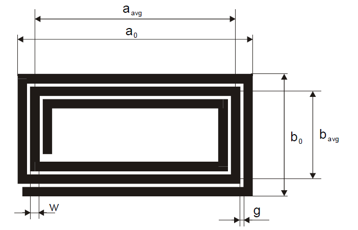
where:
- a0 & b0 are the overall dimensions of the antenna (m)
- aavg & bavg are the average dimensions of the antenna (m)
- t is the track thickness (m)
- w is the track width (m)
- g is the gap between the tracks (m)
- Nant is the number of turns
- d is the equivalent diameter of the track (m)
For this specific geometry, the equivalent inductance Lant is given by the formula:

where:


To make calculations easier, I created an excel-based calculation tool that automatically computes the equivalent inductance of the antenna according to the different geometrical parameters. This file saved me a lot of time and efforts to find the right antenna geometry.
I had an equivalent inductance Lant = 2,76 μH (close enough) with the following parameters:
- a0 = 50 mm
- b0 = 37 mm
- t = 34,79 µm (1oz)
- w = 0,3 mm
- g = 0,3 mm
- Nant = 5
If you are allergic to mathematics and calculations, other methods exist and are detailed in the following steps. It is still important to go through the calculations to learn more about basics of antenna design ;)
Attachments
Step 6: Defining the Antenna Shape : Online Calculators (2nd Method)
An alternative to long calculations endured in the previous step is the existence of online antenna geometry calculators. These calculators are made by individuals or professionals, and are intended to simplify the design of antennas. As it is difficult to verify what calculations are done by these online calculators, it is highly recommended to use calculators that show references and formulas used, or those developed by specialized companies.
STMicroelectronics offers such a calculator in its online application eDesignSuite to help customers integrate ST products into their circuit. The calculator is valid for any application with NFC technology, and can therefore be used for the NFC chip from NXP.
With the geometric values previously calculated, the resulting inductance computed by the eDesignSuite application is 2,88 μH instead of the expected value of 2,76 μH. This difference is surprising and questions the result obtained previously. The formula used by the application is unknown and it is impossible to make the comparison with the calculations done previously.
So, which of the two methods gives a correct result ?
None ! Online calculators and formulas are theoretical tools for approximating a result, but must be completed by simulations with specialized softwares and real tests in order to obtain the expected result.
Fortunately, NFC solutions already simulated and tested have been made available to electronics designers, and are the subject of the next step...
Step 7: Defining the Antenna Shape : Open Source Antennas (3rd Method)
To facilitate the implementation of their NFC ICs, some manufacturers provide complete solutions for electronics designers, such as design guides, application notes and even EDA files.
This is the case of NXP, which offers for its range of NFC integrated circuits NTAG a complete guide including references for NFC antenna design, excel-based calculation tool for rectangular and round antennas, gerber and Eagle files for different antenna classes.
A class defines the shape and size factors of an antenna. The bigger the class, the smaller the antenna. For the NFC, NXP recommends to use “Class 3”, “Class 4”, “Class 5” or “Class 6” antennas.
I decided to focus on class 4 rectangular antennas, the size of which seemed adapted for my business card, which shall be located within a zone defined either:
- External rectangle: 50 x 27mm
- Internal rectangle: 35 x 13mm, centered in the external rectangle, with 3mm corner radius
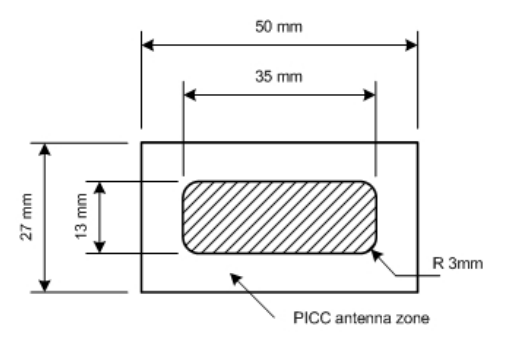
For this class, NXP provides the Eagle files of an antenna made by their engineers and already integrated in some of their products. The main advantage of this design is that it has already been simulated, corrected and fully optimized. Test methods, corrections and optimizations are presented in a document also available.
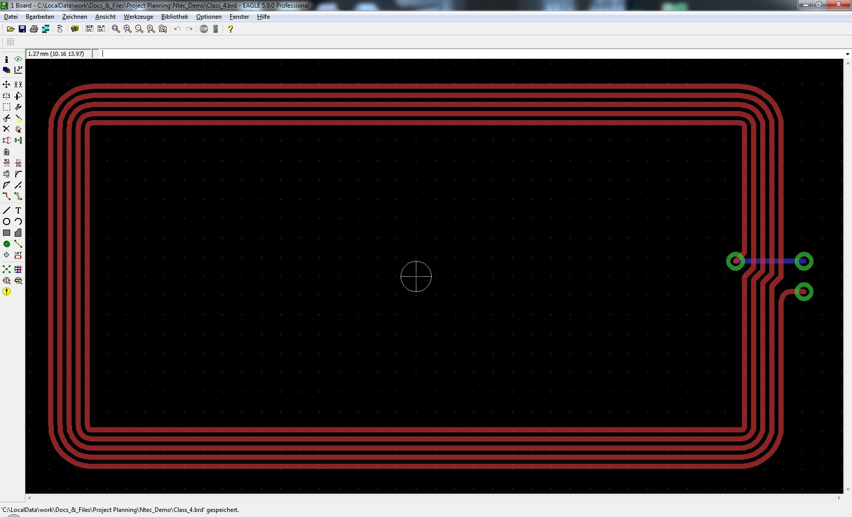
I decided to use this open source design as a model, and create my own version to implement it in a library dedicated to the project.
Attachments
Step 8: Creating the Eagle Librairy
In order to draw the electronic circuit of the business card on Eagle, it is necessary to have the symbols and fingerprints of the components used. Only the antenna and the NFC tag were missing, so I had to create them and include them in a library for the project.
I started by designing the antenna by copying the rectangular open-source class 4 antenna provided by NXP. I only changed the position of the connectors and placed them on the length of the antenna. Then, I associated the package with the symbol of a coil and added the name and value labels:
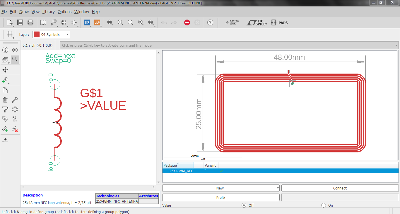
Next, I designed the NFC chip using the data provided in its datasheet. I named, sized and put together the 8 pins of the components to form the 1,6 * 1,6 mm footprint of the XQFN8 package. Finally, I associated the package with the symbol of the NTAG and added the name and value labels:

For more information on Eagle libraries and component creation, Autodesk provides tutorials on its website.
Attachments
Step 9: Schematic
The creation of the electronic schema is done on EAGLE PCB.
After importing the library "PCB_BusinessCard.lbr" created previously, the different electronic components are added to the schematic.
The NFC NT3H1101 integrated circuit, the only active component of the circuit, is connected to the passive components using the descriptions of its pins given in its datasheet:
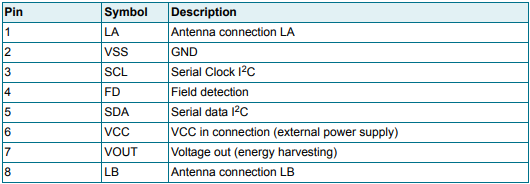
- The loop antenna of 2,75 μH is connected to LA and LB pins.
- The energy harvesting output VOUT is used to power the NFC chip and is therefore connected to its VCC pin.
- A 220 nF capacitor is connected between VOUT and VSS to guarantee operation during RF communication.
- Finally, the LED and its series resistor are powered by VOUT.
The value of the LED resistance is calculated with the ohm's law according to the parameters of the LED and the supply voltage:

where:
- R is the resistance (Ω)
- Vcc is supply voltage (V)
- Vled is the LED forward voltage (V)
- Iled is the LED forward current (A)

Attachments
Step 10: PCB Design: Bottom Face
For the design of my business card, I wanted to achieve something sober but that can show how inventive I am in life and always with a new idea in mind. I chose the design of the incandescent light bulb, symbol of a new idea whose light can illuminate the gray areas of a problem. I also liked the fact that a recruiter could easily associate my LinkedIn profile appearing on his phone with a new good idea for his company.
I started by designing a radiating light bulb on the vector drawing software Inkscape. The drawing is exported in two BitMap files, the first containing only the bulb and the second only the light rays.
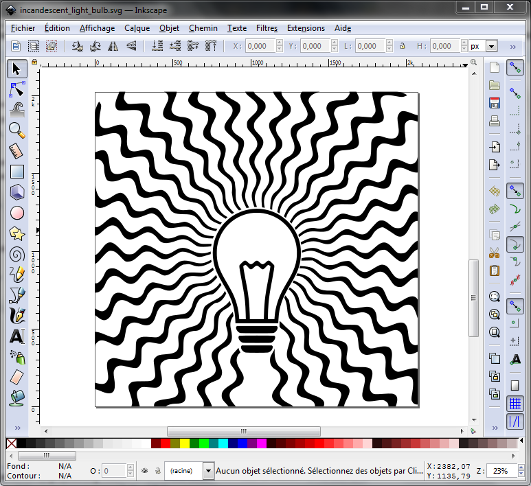
Back to Eagle, I used the import-bmp ULP in order to import the BitMap images generated by Inkscape into an Eagle drawing. This ULP generates a SCRIPT file that draws small rectangles of successionnal pixels with identical color which combined, recreate the image.
- The design of the light bulb is imported on the 22nd layer "bPlace" and will appear on the silkscreen of the PCB in white, above the black solder mask.
- The drawing of the light rays is imported on the 16th layer "Bottom" and will be considered as a copper track covered by the black solder mask.
Using the copper layer for an image allows to play with the PCB thickness and thus create texture and color effects that are normally impossible on a PCB. Artistic boards can be done with such tricks and I've been highly inspired by some pcb-art projects.
Finally, I drew the contours of the circuit and added my motto "Always a new idea." on the 22nd layer "bPlace".
Attachments
Step 11: PCB Design: Top Face
As the top face of the board is devoid of components, I was free to find an elegant way to mark my classic contact information: last name, first name, title, email and phone number.
Once again, I played with the different layers of the PCB: I started by defining a partial ground plane. Then, I imported a text containing my contact information on the 29th layer "tStop", which controls the solder mask for the top face. The superposition of the ground plane and the text on the "tStop" layer causes the letters to appear on the ground plane without the solder mask on it, giving the text a nice shiny metallic aspect.
But why not put the ground plane on the whole business card?
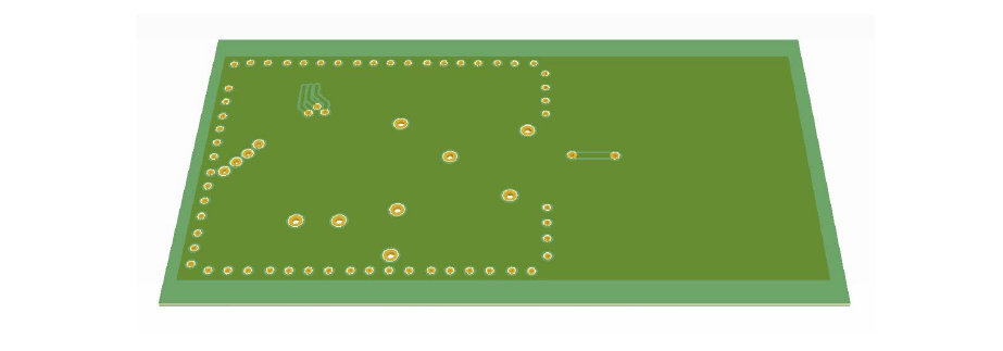
The layout of an inductive antenna on a PCB requires a special attention as radio waves can not go through metals, and there must be no copper planes above or below the antenna.
The following example shows a good implementation, where the energy transfer and the communication between the reader and the NFC tag are suitable because no copper planes overlap the antenna.

The following example shows a bad implementation, where the electromagnetic flux cannot flow through the antenna. The ground plane on one side of the PCB blocks the energy transfer between the reader and the NFC tag antenna:
Step 12: PCB Routing
I started by placing all the different components on the bottom face of the PCB.
The LED is placed on the light bulb filament, and the other components are arranged in the most discreet manner possible at the base of the light bulb.
The wires connecting the different passive components to each other or to the NFC tag are preferably placed under the lines drawing the bulb for aesthetic reasons.
Finally, the antenna is placed at the bottom of the circuit, around the motto, and connected to the NFC integrated circuit by two thin wires.
The PCB design is now done !
Attachments
Step 13: Generating the Gerber Files
Gerber files are the standard file used by printed circuit board industry software to describe the PCB images: copper layers, solder mask, legend, etc...
Whether you choose to manufacture your PCB at home or entrust the manufacturing process to a professional, it is essential to generate the Gerber files from the PCB previously made on Eagle.
Exporting Gerber files from Eagle is very simple using the in built CAM processor: I used the CAM file for Seeed Fusion 2-layers PCB which contain all settings used by this manufacturer and many others. More informations about Gerber generation with this file can be found on Seeed's website.
The CAM processor generates a .zip file "NFC_BusinessCard.zip" containing 10 files corresponding to the following layers of the NFC Business Card PCB:
| Extension | Layer |
|---|---|
| NFC_BusinessCard.GBL | Bottom Copper |
| NFC_BusinessCard.GBO | Bottom Silkscreen |
| NFC_BusinessCard.GBP | Bottom Solder Paste |
| NFC_BusinessCard.GBS | Bottom Soldermask |
| NFC_BusinessCard.GML | Mill Layer |
| NFC_BusinessCard.GTL | Top Copper |
| NFC_BusinessCard.GTO | Top Silkscreen |
| NFC_BusinessCard.GTP | Top Solder Paste |
| NFC_BusinessCard.GTS | Top Soldermask |
| NFC_BusinessCard.TXT | Drill File |
To be sure that the PCB will look exactly as I wanted, I uploaded the Gerber files in EasyEDA's online Gerber viewer. I changed the theme to black and the surface finish to silver to visualize the final design after fabrication.
I was really happy with the result and decided to go on with the manufacturing step...
Attachments
Step 14: Ordering the PCBs
As I wanted a quality finish for my business cards, I entrusted the manufacturing process to a professional.
Many PCB manufacturers now offer very competitive prices: SeeedStudio, Elecrow, PCBWay, and many others... Tip: To compare prices and services offered by different PCB manufacturers, I advise to use the PCB Shopper website which I find very handy.
For the fabrication of my business cards, I took into account an important detail: many PCB manufacturers allow themselves to mark the order number on the PCB silkscreen. This number, although small, is annoying especially when the PCB needs to be aesthetic. For example, I had this bad surprise for my $1 PCB Christmas Trees, ordered on SeeedStudio.
From experience, I knew that Elecrow did not have this bad habit and so I decided to entrust the fabrication of my cards to this manufacturer and I ordered 10 business cards for $4.9 with the following settings:
- Layers: 2 layers
- Dimensions: 54*86 mm
- Different PCB Design: 1
- PCB Thickness: 0,6 mm (the thinnest available)
- PCB Color: Black
- Surface Finish: HASL
- Castellated Hole: No
- Copper Weight: 1oz (as chosen in the antenna inductance formula)
Two weeks later, I received my PCBs perfectly made and without any annoying order number marked on the silkscreen. So far so good, time to solder these boards!
Step 15: Soldering the NFC Chip
The hand soldering of the NFC integrated circuit is without a doubt one of the most difficult steps of this project: the XQFN8 package of 1.6 * 1.6 mm makes the task difficult but not impossible.
I started by taking a small amount of solder flux with a toothpick, and put it on the footprint of the integrated circuit: the flux acts as a temporary glue and allows to properly place the component.
Once the integrated circuit correctly placed and aligned on its footprint, I used cross-lock tweezers to secure the component to the PCB.
Then, I took a small amount of solder paste with the other end of the toothpick, and put it on the pins of the chip.
I used a hot air rework tool to melt the solder paste and solder the pins of the integrated circuit to the circuit tracks. The result is a huge weld ball shorting the pins of the tag because of too much solder paste. To remove excess solder, I used a conventional soldering iron and solder flux.
Once the excess of solder removed, it can be seen under the solder flux deposits that the component is properly soldered.
I finally removed solder flux spots and cleaned the business card with a Q-tip and isopropyl alcohol.
Step 16: Soldering the Passive Components
I started the passive components soldering with the 0603 capacitor: to solder the capacitor, I first began by placing a small amount of solder on one of its pad. Then, I approached the capacitor with fine tweezers while keeping the solder molten with my soldering iron. Once the capacitor correctly placed, I removed my soldering iron to solidify the solder. The second pad soldering can then be made without the need to hold the capacitor with the tweezers.
I repeated the same process for the resistor and the LED.
Once the three passive components, I finally removed solder flux spots and cleaned the business card with a Q-tip and isopropyl alcohol.
The business card is almost finished !
Step 17: Programming the NFC Chip
The business card is now ready to contain information to be transmitted by NFC. For the programming of this one, I used my phone and an application which can read and write tags, including this integrated circuit, using NFC:
NFC tools is an application for reading and writing NFC tags. Available for Android and iOS, it can be downloaded for free:
Step by step guide:
- Enable NFC
- On Android, by clicking on the NFC icon in the quick settings menu, or in Settings menu. Note that not all Android phones are equipped with NFC technology, although it is generally found on all recent phones.
- On iOS, NFC Tools will automatically enable NFC. Note that NFC technology is present on all Apple phones since the iPhone 6. - Start NFC Tools
- In the "Write" menu, select "Add a record"
- Choose "URL" as a record
- Enter the link you want the NFC to transfer, then click OK
- Choose "Write" to write a NFC tag
- An animated icon is displayed until you approach the business card to your phone
- The LED of the business card should lights up and the icon should says "Write complete!"
Success ! The business card is finally ready !
In the "Other" menu, some interesting features are presented such as "copy to infinity!" in order to program a lot of business cards, or "lock tag" to prevent the re-writing of the card.
Step 18: Conclusion
This project was not only fun but also challenging, as I wanted to create something that I am proud of and that can show my passion for my studies and PCB design.
I am glad to have created an electronic circuit and its PCB that not only taught me a lot about NFC technology and antenna design, but is also useful in my everyday life and for my professional career.
In parallel, I posted the demo video of my business card on my LinkedIn profile hoping for feedbacks and opinions. The result was beyond my expectations as the post became viral and I received dozens of internship proposals and meeting invitations. Thanks to my PCB business card with NFC, I found a 6 months internship in the company of my dreams !
Today, I am proud to be able to transmit through this tutorial the knowledge I gained during this project. I hope you liked it :)

Judges Prize in the
PCB Contest


