

Introduction: AVR Assembler Tutorial 7


Welcome to Tutorial 7!
Today we are going to first show how to scavenge a keypad, and then show how to use the Analog input ports to communicate with the keypad.
We will do this using interrupts and a single wire as input. We will wire the keypad so that each keypress sends a unique voltage to the analog input which will allow us to distinguish by the voltage which key was pressed. Then we will output the number pressed to our register analyzer to show that everything is happening as it should.
There are a number of pitfalls that you can run in to when using the Analog to Digital Converter (ADC) in the ATmega328p and so we will take things in a few stages on the way to try and figure out how to avoid them. We will also see why using the analog to digital converter is not the best way to control a keypad even though it does use fewer ports on your microcontroller.
In this tutorial you will need:
- a keypad. You can buy one or you can do what I did and scavenge one.
- 2 female headers for the keypad (if you are scavenging one)
- connecting wires
- a breadboard
- 4 1 Kohm resistors
- 1 15 Kohm resistor
- 1 3.3 Kohm resistor
- 1 180 ohm resistor
- 1 680 ohm resistor
- a digital multimeter
- your analyzer from Tutorial 5
You may want to skip the first few steps if you have already have a keypad and don't need to scavenge one.
Here is a link to the complete collection of my AVR assembler tutorials: https://www.instructables.com/id/Command-Line-AVR-T...
Step 1: Scavenge a Keypad 1


Long ago, when even your grandparents were mere children, people used to use these weird looking devices, that had long cables plugged into the wall, to communicate with one another. They were called "telephones" and were usually cheap plastic things that made an annoying sound when someone called you (not that the "Justin Bieber" ringtones of today aren't equally annoying). In any case, these devices had keypads on them which were very simply wired and so are easy to scavenge and they have 2 extra keys on them ("redial" and "flash")from the keypads you can buy that you may want to repurpose as "arrow keys", "menu keys", or something else.
So we are going to start by scavenging a keypad from an old phone.
First take the phone (I use a GE one as shown in the pictures) and pry it apart to reveal the wiring.
Then take a chisel and snap off the little plastic knobs that are holding the keypad on and remove the keypad.
Step 2: Scavenge a Keypad 2


Now take a PVC saw and cut the plastic from around the keyholes and then cut around the edge to get the depth right leaving a thin keypad.
Then put the keypad back on using the little pegs that remain after you clipped the tops off of them in the last step and use a soldering iron to simply poke the hot iron into each peg hole which will melt the plastic and spread it out over the bottom of the keypad forming new "knobs" which will hold the keypad in place as before.
I like to scavenge the three speakers and maybe the other things like switches and what-not that are on the board. However, this time I am not going to scavenge the switches and stuff because we have other goals at the moment. Also, there is a TA31002 linear IC in there which is a telephone ringer. The datasheet is easily found and downloaded online giving the pinout and features. So I am going to leave it soldered to the board for now and then play around with it later. I would like to hook it up to an oscilloscope and see what cool signals I can get out of it. Maybe even make a doorbell out of it. Who knows.
Anyway once you are finished destroying the phone and scavenging the parts we will finish making our keypad.
Step 3: Scavenge a Keypad 3


Use a desoldering wick and remove the ribbon cables from the bottom of the keypad making sure that the holes in the circuit board are clear and then attach two female headers onto the board where the holes are. You will probably have to clip down your headers so that they are 4-pin headers.
Now that the headers are attached you can wire it to a breadboard, take a multimeter, and test the keys by sticking the multimeter across random pins and measuring the resistance. This will allow you to map out the keys. It is difficult to see how the keys are wired to the outputs by looking at the circuit but if you use a multimeter you can plug it in to any two pins and then press buttons until you see a number on the screen instead of an open circuit. This will be the pinout for that key.
Map all of the keys to output pins in this way.
Step 4: Wire the Keypad


Now follow the wiring diagram and wire the keypad to your breadboard.
How this is going to work is we will put 5V in to the left hand side and the right side goes to GND. The first pin on the right in the diagram goes into the first of our analog pins on the Atmega328p microcontroller. When there are no buttons pressed the signal will be 0V, and when each of the different buttons are pressed the input to the analog port will range between 0V and 5V with a different amount depending on which key was pressed. We chose the resistor values so that each path would contain a resistance that was different from the rest. The analog port on the microcontroller takes an analog signal and splits it into 1024 different channels between 0V and 5V. This means that each channel has a width 5V/1024 = 0.005 V/channel = 5 mV/channel. So the analog port can distinguish input voltages as long as they differ by more than 5 mV. In our case we have chosen resistor values so that any two keypresses will send a voltage signal that differ by more than this so the microcontroller should easily be able to decide which key was pressed. The big problem is that the whole system is very noisy so we will need to choose a range of voltages to map to each button press -- but we will get in to that a bit later.
Notice that we are able to control a 14 button keypad using only a single input line to the controller. That is one of the useful aspects of analog inputs.
Now our first attempt at controlling the keypad will be to have a keypress cause an interrupt, the interrupt subroutine will read the analog input port and decide which key was pressed, and then it will output that number to our register analyzer subroutine which will display the key value in binary on our 8 LEDs which we set up in Tutorial 5.
Step 5: Wire the Keypad to Your Analyzer
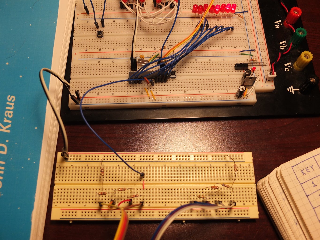

The pictures show how we want to wire the keypad to the microcontroller so that we can see the output on our analyzer display. Essentially we simply wire the output from the keypad to PortC pin 0, which is also called ADC0 on the ATmega328P.
However, there is a couple additional things. We are also going to wire a button to PD2. I.e. take a wire from your 5V rail to a button and from the other side of the button to PD2, and lastly, we want to disconnect the AREF pin from our 5V rail and instead leave it disconnected. We could insert a 0.1 microfarad decoupling capacitor if we wanted. This is a ceramic capacitor with a 104 written on it. The first two digits are the number and the last digit is the power of 10 we multiply it by to get an answer in picofarads (pico means 10^-12), So 104 means 10 x 10^4 picofarads, which is the same as 100 nanofarads (nano means 10^-9), which is the same as 0.1 microfarads (micro means 10^-6). Anyway, all this does is stablize the AREF pin when we can use it as our reference pin.
We also want a 1 Mohm resistor between PD2 and ground. We are going to set PD2 as an output pin at 0V and we will be triggering on a positive edge at that pin. We want the edge to disappear immediately when we release the button so we will insert this "pull down" resistor.
The reason that we want the button is because we want to trigger our Analog-to-Digital converter off of pin INT0 on the chip, which is also PD2. Eventually we would like the keypress to both trigger the ADC and also provide the input to be converted without having a separate button, but because of the way the timing works we will begin by having a separate button to trigger the ADC and once we iron all the bugs out and are confident that everything is working properly, then we will tackle the noise and timing issues that come with triggering from the same button press that we want to read.
So, for now, the way it works is we will hold down a key, then push the button to trigger the ADC, and then let go and hopefully the binary value of the button we pushed will show up on the analyzer.
So let's write some code that will accomplish that.
Step 6: Which Toggle Switches Should We Set?

Let's first think about how we are going to code this so that the controller can read the input from the keypad and turn it into a numerical value corresponding to the button which was pressed.
We are going to use the Analog to Digital Converter (ADC) that is built in to the Atmega328p. We will be using AREF as our reference voltage and our keypad output will be connected to PortC0 or PC0. Note that this pin is also called ADC0 for Analog-to-Digital Converter 0.
It might be a good idea for you to read through Section 12.4 on interrupts for the ATmega328P and also chapter 24 on the Analog-to-Digital Converter before we get started or at least have those sections ready for reference.
In order to set up the microcontroller so that it knows what to do with an analog input signal, and how to interact with our program, we first have to set a few of the various ADC related register bits. These are essentially equivalent to the old toggle switches on the first computers. You either flip a switch ON or OFF, or even further back you would plug in cables between one outlet and another so that electrons reaching that fork in the road would find one gate closed and another open forcing it down a different path in the maze of circuitry and thus performing a different logical task. When coding in assembly language we have close access to these functions of the microcontroller which is one of the attractive things about doing it in the first place. It is more "hands on" and far less is going on "behind the scenes" as it were. So don't think of setting these registers as a tedious task. This is what makes assembly language interesting! We are gaining a very personal relationship with the inner workings and logic of the chip and making it do exactly what we want it to -- no more and no less. No wasted clock cycles.
So here is a list of the switches we need to set:
- Turn off the Power Reduction ADC bit, PRADC, which is bit 0 of the PRR register, since if this bit is on it will shut down the ADC. The power reduction register is essentially a way to shut off various things that use power when you don't need them. Since we are using the ADC we want to make sure it is not disabled in this way. (See PRADC on page 46)
- Select the analog input channel to be ADC0 by turning off MUX3...0 in the ADC Multiplexer Selection (ADMUX) register (See table 24-4 page 249) these are already off by default so we don't really need to do this. However, I am including it since if you ever use a port other than ADC0 you will need to toggle these switches accordingly. Various combinations of MUX3, MUX2, MUX1, MUX0 allow you to use any of the analog ports as your input and you can also change these on the fly if you want to look at a bunch of different analog signals at once.
- Turn off REFS0 and REFS1 bits in the ADMUX register so that we will use AREF as our reference voltage rather than an internal reference (See page 248).
- Turn on the ADLAR bit in ADMUX so the result is "left adjusted" we will discuss this choice in the next step.
- Set the ADC0D bit in the Digital Input Disable Register (DIDR0) to turn off digital input to PC0. We are using that port for analog input so we might as well disable the digital input for it.
- Set ISC0 and ISC1 in the External Interrupt Control Register A (EICRA) to indicate that we want to trigger on the rising edge of a voltage signal to the INT0 pin (PD2), see page 71.
- Clear bits INT0 and INT1 in the External Interrupt Mask Register (EIMSK) to indicate that we are not using interrupts on this pin. If we were to enable interrupts on this pin we would need an interrupt handler at address 0x0002 but instead we are setting it up so that a signal on this pin triggers the ADC conversion, the completion of which is handled by the ADC conversion complete interrupt at address 0x002A. See page 72.
- Set the ADC Enable (ADEN) bit (bit 7) in the ADC control and status register A (ADCSRA) to enable the ADC. See page 249.
- We could start a single conversion by setting the ADC start conversion bit (ADSC) each time we wanted to read the analog signal, however, for now we would rather have it read automatically whenever somebody pushes the button, so instead we will enable the ADC Autotrigger Enable (ADATE) bit in the ADCSRA register so that triggering is done automatically.
- We also set the ADPS2..0 bits (the AD Prescalar bits) to 111 so that the ADC clock is the CPU clock divided by a factor of 128.
- We will select the source of the ADC triggering to be PD2 which is also called INT0 (External Interrupt Request 0). We do this by toggling the various bits in the ADCSRB register (See Table 24-6 on page 251). We see by the table that we want ADTS0 off, ADTS1 on, and ADTS2 off so that the ADC will trigger off that pin. Note if we wanted to continuously sample the analog port like if we were reading some continuous analog signal (like sound sampling or something) we would set this to Free Running Mode. The method we are using of setting triggering on PD2 triggers an ADC reading of the analog port PC0 without causing an interrupt.The interrupt will come when the conversion is complete.
- Enable the ADC Interrupt Enable (ADIE) bit in the ADCSRA register so that when the analog to digital conversion is complete it will generate an interrupt which we can write an interrupt handler for and put at .org 0x002A.
- Set the I bit in SREG to enable interrupts.
Exercise 1: Make sure you read the relevant sections in the datasheet for each of the above settings so that you understand what is going on and what would happen if we changed them to alternate settings.
Step 7: Write the Interrupt Handler
In the last step we saw that we have set it up so that a rising edge detected on PD2 will trigger an analog to digital conversion on PC0 and when this conversion is complete it will throw an ADC Conversion Complete interrupt. Now we want to do something with this interrupt.
If you examine Table 12-6 on page 65 you will see a list of the possible interrupts. We have already seen the RESET interrupt at address 0x0000 and the Timer/Counter0 Overflow interrupt at address 0x0020 in previous Tutorials. Now we want to look at the ADC interrupt which we see by the table is at address 0x002A. So at the beginning of our assembly language code we will need a line that reads:
.org 0x002A
rjmp ADC_int
which will jump to our interrupt handler labeled ADC_int whenever the ADC has completed a conversion. So how should we write our interrupt handler?
The way that the ADC works is by performing the following calculation:
ADC = Vin x 1024 / Vref
So let us see what happens if I push the "redial" button on the keypad. In that case the voltage on PC0 will change to some value, say 1.52V, and since Vref is at 5V we will have:
ADC = (1.52V) x 1024 / 5V = 311.296
and so it would show up as a 311. If we wanted to convert this back to a voltage we would just reverse the calculation. We won't need to do this however since we are not interested in the actual voltages just in distinguishing between them.
When the conversion is finished, the result is stored in a 10-bit number placed in ADCH and ADCL registers and we have caused it to be "left adjusted" which means that the 10-bits start at bit 7 of ADCH and go down to bit 6 of ADCL (there are 16 bits total in these two registers and we only use 10 of them, i.e. 1024 channels). We could have the result "right adjusted" if we wanted by clearing the ADLAR bit in the ADMUX register.The reason we choose left adjusted is because our signals are far enough apart that the last two digits of the channel number aren't relevant and are probably just noise so we will distinguish the keypresses using only the upper 8 digits, in other words, we will only need to look at ADCH to figure out which button was pressed.
So our interrupt handler should simply read the number out of the ADCH register, convert that number into a keypad value, and then send that value to our register analyzer LED's so that we can verify that pushing a "9" say, will cause the LED's corresponding to "00001001" to light up.
Before we go that far though we need to first see what shows up in ADCH when we push the various buttons. So let's just write a simple interrupt handler that just sends the contents of ADCH to the analyzer display.
So here is what we need:
ADC_int:
lds analyzer, ADCH ;load the value of ADCH into our analyzer
sbi EIFR,0 ; clear the external interrupt flag so that it is ready to go again
reti
By now, you should be able to just copy the code from our analyzer in tutorial 5 and add this interrupt and the toggle settings and run it.
Exercise 2: Write the code and run it. See that you get the ADCH displaying on your analyzer display. Try pushing the same keypress multiple times. Do you always get the same value in ADCH?
Step 8: Map Out the Keypress Values

What we need to do now is convert the values in ADCH into numbers corresponding to the key that was pressed. We do this by writing out the contents of ADCH for each keypress and then converting that into a decimal number like I did in the picture. In our interrupt handling routine we will consider a whole range of values as corresponding to each keypress so that the ADC will map anything in that range to a given keypress.
Exercise 3: Do this mappng and then re-write your ADC interrupt routine.
Here is what I got for mine (yours will very likely be different). Notice that I have set it up with a range of values for each keypress.
ADC_int:         ; External interrupt handler
clr analyzer     ; prepare for new number
lds buttonH,ADCH ; ADC updates when ADCH is read clc
cpi buttonH,240
brlo PC+3        ; if ADCH is bigger then it's a 1
ldi analyzer,1   ; so load analyzer with a 1
rjmp return      ; and return clc
cpi buttonH,230  ; if ADCH is bigger then a 2
brlo PC+3
ldi analyzer,2
rjmp return clc
cpi buttonH,217
brlo PC+3
ldi analyzer,3
rjmp return clc
cpi buttonH,203
brlo PC+3
ldi analyzer,4
rjmp return clc
cpi buttonH,187
brlo PC+3
ldi analyzer,5
rjmp return clc
cpi buttonH,155
brlo PC+3
ldi analyzer,6
rjmp return clc
cpi buttonH,127
brlo PC+3
ldi analyzer,255 ; we will set flash as all on
rjmp return clc
cpi buttonH,115
brlo PC+3
ldi analyzer,7
rjmp return clc
cpi buttonH,94
brlo PC+3
ldi analyzer,8
rjmp return clc
cpi buttonH,62
brlo PC+3
ldi analyzer,9
rjmp return clc
cpi buttonH,37
brlo PC+3
ldi analyzer,0b11110000 ; asterisk is top half on
rjmp return clc
cpi buttonH,28
brlo PC+3
ldi analyzer,0
rjmp return clc
cpi buttonH,17
brlo PC+3
ldi analyzer,0b00001111 ; hash sign is bottom half on
rjmp return clc
cpi buttonH,5
brlo PC+3
ldi analyzer,0b11000011 ; redial is top 2 bottom 2
rjmp return
ldi analyzer,0b11011011 ; otherwise error occurred return:
reti
Step 9: Code and Video for Version 1
I have attached my code for this first version of the keypad driver. In this one you need to push the key and then push the button in order to cause the ADC to read the input from the keypad. What we would rather have is no button but instead the signal to do the conversion comes from the keypress itself.
Exercise 3: Assemble and upload this code and try it. You may have to change the various conversion thresholds to correspond to your keypress voltages since they likely differ from mine. What happens if you try to use an input from the keypad both for the ADC0 and for the external interrupt pin instead of through a button?
I will also attach a video of the operation of this first version of our keypress driver.
You will notice that in my code there is a section initializing the Stack Pointer. There are various registers that we may want to push and pop from the stack when we are manipulating variables and what-not and there are also registers that we may want to save and restore later. For example, SREG is a register that is not preserved across interrupts, so the various flags that are set and cleared as a result of operations may be changed if an interrupt occurs in the middle of something. So it is best if you push SREG on to the stack at the beginning of an interrupt handler and then pop it off again at the end of the interrupt handler. I have placed it in the code to show how it is initialized and to anticipate how we will need it later but since we don't care what happens to SREG during interrupts in our code I didn't use the stack for this.
Also notice that I have used the shift operation to set various bits in registers when initializing. For example in the line:
ldi temp,(1<<ISC01)|(1<<ISC00)   ; comment to fix Instructables formating issues: >>>>
sts EICRA,temp
The "<<" command in the first line of code above is a shift operation. It essentially takes the binary number 1, which is 0b00000001 and shifts it left by the amount of the number ISC01. This is the position of the bit named ISC01 in the EICRA register. Since ISC01 is bit 1, the number 1 is shifted to the left 1 position to become 0b00000010. Similarly the second, ISC00, is bit 0 of EICRA and so the shift of the number 1 is zero positions to the left. If look take another look at the m328Pdef.inc file that you downloaded in the first tutorial and have been using evrr since, you will see that it is just a long list of ".equ" statements. You will find that ISC01 is equal to 1. The assembler replaces every instance of it with 1 before even starting to assemble anything. They are just names for register bits to help us humans read and write code. Now, the vertical line between the two shift operations above is a logical "or" operation. Here is the equation:
0b00000010 | 0b00000001 = 0b00000011
and this is what we are loading (using "ldi") into temp. The reason people use this method to load values into a register is that it allows one to use the name of the bit instead of just a number and this makes the code is much easier to read.
There are also two other techniques we have used. We use the instructions "ori" and "andi". These allow us to SET and CLEAR bits respectively without changing any of the other bits in a register. For example, when I used
ori temp,(1<ADC0D) ; comment to fix formating: >
this "or"s temp with 0b00000001 which puts a 1 in the zeroth bit and leaves all the rest unchanged. Also when we wrote
andi temp,0b11111110
this changes the zeroth bit of temp to a 0 and leaves all the rest unchanged.
Exercise 4: You should go through the code and make sure you understand each line. You may find it interesting to find better methods for doing things and write a better program. There are a hundred ways to code things and I am pretty confident you can find a much better way than mine. You may also find (heaven forbid!) errors and omissions. In that case I would sure like to hear about them so they can be fixed.
Okay, now let's see if we can get rid of that superfluous button...
Attachments


Step 10: Code for Version 2
The simplest way to get rid of the button is just to remove it altogether, forget the input to PB2, and just switch the ADC to "Free Running Mode".
In other words simply change the ADCSRB register so that ADTS2, ADTS1, and ADTS0 are all zero's.
Then set the ADSC bit in ADCSRA to 1 which will start the first conversion.
Now upload it to your microcontroller and you will find that the correct number comes up on the display while you are pressing the button and only while you are pressing the button. This is because the ADC is continuously sampling the ADC0 port and displaying the value. When you take your finger off of the button, the "button bounce" will cause a few random values to occur very quickly and then it will settle back to 0V input. In our code we have this 0V appearing as 0b11011011 (because the keypress `0' is already using the 0b00000000 display value)
This is not the solution we want though for two reasons. First we don't want to have to hold the button. We want to press it once and have the number displayed (or used in some new code in a later tutorial). Secondly, we don't want to continually sample the ADC0. We want it to take a single reading, convert it, and then sleep until a new keypress triggers a new conversion. Free running mode is best if the only thing you want the microcontroller to do is continually read some analog input -- like if you wanted to display real time temperatures or something.
So let's find yet another solution...
Attachments
Step 11: How Do We Get Rid of the Button? Version 3

There are numerous ways we could proceed. First we could add hardware to get rid of the button. For example we may try putting a transistor in the circuit at the output line of the keypress so that it would take a small trickle of the current from the output and send a 5V pulse to the interrupt pin PD2.
However, that would probably be too noisy at the least and at worst it wouldn't allow enough time for an accurate keypress reading since the voltage output of the keypad wouldn't have time to stabilze before the ADC reading is captured.
So we would rather come up with a software solution. What we would like to do is add an interrupt on the PD2 pin and write an interrupt handler for it which calls a single reading of the keypad pin. In other words, we get rid of the autotrigger interrupt from the ADC, and add an external interrupt that calls the ADC inside it. That way the signal to read the ADC comes after the PD2 signal has already occurred and this might give things enough time to stablize to an accurate voltage before the PC0 pin is read and converted. We would still have an ADC completion interrupt which outputs the result to the analyzer display at the end.
Make sense? Well let's do it...
Take a look at the new code attached.
You see the following changes:
- We added a rjmp at address .org 0x0002 to handle the INT0 external interrupt
- We changed the EIMSK register to indicate we want to interrupt on the INT0 pin
- We changed the ADATE pin in the ADCSRA register to disable autotriggering
- We got rid of the ADCSRB settings since they are irrelevant when ADATE is off
- We no longer have to reset the external trigger flag since the INT0 interrupt routine does this automatically when it completes -- previously we didn't have an interrupt routine, we just triggered the ADC off of a signal at that pin, so we had to clear that flag by hand.
Now in the interrupt handler we simply call a single conversion from the ADC.
Exercise 5: Run this version and see what happens.
Attachments
Step 12: Code and Video for the Working Version
As we saw by the last version, the button interrupt doesn't work very well because the interrupt is triggered on a rising edge to pin PD2 and then the interrupt handler calls the ADC conversion. However, the ADC then gets the voltage reading before it has stabilized and so it reads nonsense.
What we need is to introduce a delay between the interrupt on PD2 and the ADC reading on PC0. We will do this by adding a timer/counter, a counter overflow interrupt, and a delay routine. Luckily we already know how to do this from Tutorial 3! So we will just copy and paste the relevant code from there.
I have given the resulting code and a video showing it in operation.
You will notice that the readings are not as accurate as one would hope. This is likely because of a number of sources:
- we are tapping from the voltage output of the keypad to trigger on PD2 which affects the reading in PC0.
- we don't really know how long to delay after the trigger to get the best reading.
- it takes a few cycles for the ADC conversion to complete which means that we can't rapid fire on the keypad.
- there is probably noise in the keypad itself.
- etc...
So, although we managed to get the keypad to work, and we could now use it in applications by using the keypress values in some other way instead of just outputting them to the analyzer display, it is not very accurate and it is very annoying. That is why I think that the best way to wire keypads is simply to stick each output from the keypad into a different port and decide which key is pressed by which ports see a voltage. That is easy, very fast, and very accurate.
In fact, there are only two reasons why one would want to drive a keypad the way we have done here:
- It only uses 2 of the pins on our microcontroller instead of 8.
- It is a great project to show different aspects of the ADC on the microcontroller which is different from the standard things you can find out there like temperature readings, turning potentiometers, etc. I wanted an example of triggered single readings and external pin auto-triggering rather than just free running CPU-gobbling mode.
Anyway, here is a final couple of exercises for you:
Exercise 6: Re-write the ADC conversion complete interrupt handler to use a Look-up Table. I.e. So that it tests the analog value with the first item in the table and if it is bigger it returns from the interrupt, if it is not then it increments Z to the next item in the table and branches back to the test again. This will shorten the code and clean up the interrupt routine and make it look nicer. (I will give a possible solution as the next step)
Exercise 7: Hook up your keypad to 8 pins on the microcontroller
and write the simple driver for it and experience how much nicer it is. Can you think of a few ways of making our method work better?
That is all for this tutorial. I have attached the final version with pointers. As we make our way closer to our final goal, we will use the keyboard once more in Tutorial 9 to show how to control seven segment displays with it (and building something interesting that uses the extra keys on the phone keypad) and then we will switch to controlling things with button-presses instead (since that method fits better with the end product we are building toward with these tutorials) and we will just shelve the keypad.
See you next time!
