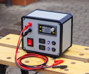
Introduction: Home Lab Voltage Reference Module


If you've ever worked with the ADC of an Arduino you've probably discovered that the readings aren't accurate at all. And it gets even worse about it's rated temperature range.
There are many reasons for this, but one of the main causes is within the way an ADC operates. It can not measure a voltage on its own, but only compare it with another voltage. The Arduino offers you to choose from an internal 1.1V, the AVCC system voltage as this reference voltage or an external voltage input.
Unfortunately the first two ans simple solutions are far from perfect. The internal reference has an initial accuracy of 10% and an unspecified behavior over the temperature range. The AVCC voltage heavily depends on the used regulator, the capacitors used, the board layout, other load on the same rail and much more.
The simple solution is to use a specific external reference IC to generate an precise voltage. This voltage can be feed into the AREF input of the Ardino or any other ADC/DAC for that matter. Those chips can be manufactured with incredible tight voltage tolerances of down to 0.02% and with a temperature drift down to 1ppm (0.0001% change per °C). With that spec they can be used to calibrate basically anything, from an Arduino to your multimeter!
As those chips can get fairly pricey I wanted to be able to re-use them for any future project and thus designed a small adapter board. While I was on it I added plenty of protection, additional smoothing and out-of-spec outputs.
Step 1: Features
- small, re-usable DIP-20 package
- up to 16V input voltage
- extended operating temperature range: -40 - 125°C (only limited by reference chip)
- low cost, cheaper than the reference IC in most cases
- enable input
- protection against:
- over-voltage up to 18V
- reverse voltage up to -20V
- reverse insertion in DIP-20 and DIP-14 sockets
- status output
- low input voltage warning
- warm-up warning
- low temp warning
- high temp warning
- raw temperature data output
- additional 2.495V auxiliary reference
- reference stabilisation
- LDO to eliminate low frequency noise
- passive RC filter for use with switch-mode regulators
- mechanical influence reduced with 'floating' board
- customisable
- fits most SO-8 reference ICs
- supports additional noise reduction capacitors for some references
- all voltage dividers are placed on the top side
- all caps for reference are placed on the top side
- designed with common parts and footprints
Step 2: Assembly


Start by soldering wires into the top 14 holes of the socket. Be careful to not overheat the plastic as it may deform and badly fit into its socket.
Alternatively you can remove half of the large holes for the socket on the PCB to end up with "castellated vias" like in the picture above. You can either use sidecutters or a small handsaw for this job. Good PCB manufactures will do this for you, but the boards likely cost unreasonable more.
The second option is faster by may result in less durable solder joints after mounting.
This module is designed to suit multiple reference ICs. Depending on which chip (and output voltage) you choose, you need to pick the right value capacitors and resistors. Recommended values for common parts and configurations are provided in the spreadsheet as part of the → documentation. If you want to use an other reference you may want to check out the chapter → Customise.
After you figured out which values to use solder all components except the reference onto the PCB. I'd suggest to solder the fine-pitch TSSOP-14 part first since rework will be fairly easy then. Proceed with the remaining components.
The next step might be to test the module to check if everything (except the reference) is working correctly.
Now you can proceed to solder the PCB onto the socket as shown. The bottom section is designed to fit right between the plastic frame. Be sure to match the pin 1 indication (notch in the socket, square pad on the PCB).
The last step is to solder the main voltage reference onto the module. This should be done last not only because it is the most expensive part in this project, but to reduce thermal and mechanical stress as much as possible. The effects are tiny, but in comparison to the super tight tolerances it does have a rather significant influence.
Step 3: Usage

With it's standard IC sized socket this module fits easily into your standard breadboard. However this module was designed for temperature cycling so I recommend to build the circuit onto prefboard for better results.
Power Connections:
Most importantly you need to feed the module with a sufficient voltage. You need to account for the voltage drops within the reference, within the LDO and some due to the RC filter network. In most cases a voltage about 3V higher than the reference voltage will do just fine; the calculation is explained in detail in chapter → Customise.
Best Performance:
The key for good performance is to keep the reference tightly coupled to the Arduino, Atmega or any other ADC/DAC you want to use.
Connect both grounds to the ground of the ADC and the reference output to the ADC ref input with as short wires as possible. Make sure to connect the grounds only at one point, the ground pin of the ADC. These measures reduce the influence of the wiring, even the smallest amount of resistance can cause a tiny offset which ruins the superb absolute accuracy.
For a stable and "clean" signal make sure no high frequency digital signals are running nearby, for complex systems you may even add a local ground plane, connected to the ground pin of the ADC, to reduce the crosstalk even further.
Enable Input:
The module has an enable input to reduce power consumption if not needed. Make sure to connect this pin to the input pin if you want to have this module turned on at all times.
Error Outputs:
To check if the module is operating correctly there are four open-drain active-low outputs provided. There are multiple ways how you can utilize these:
1. Connect an LED with a resistor in series to any of the outputs and and a positive voltage. Make sure the cathode (-) of the LED is connected to the output. If this error occurs the LED will start to light.
2. Connect any of the outputs to a digital input of the Arduino and enable it's internal pull-up resistor. Whenever this error occurs the input will read '0', if everything is on it will read '1'.
3. If you don't need to monitor every output individually it is possible to connect multiple outputs in parallel without any additional circuitry. If you haven't worked with open-drain outputs yet, you can imagine it as if multiple buttons are connected in parallel.
Temperature Output:
While it is mainly used for on-board supervision you can also read out the temperature of the TC1047A temperature sensor manually with an Arduino or any other microcontroller, you can even use a simple multimeter.
Auxiliary Reference Output:
A second 2.495V reference voltage is generated for the on-board supersision circuitry, but it may also be used for external circuitry. Make sure the external circuitry draws less than 1mA at all times.
The picture above is an example how an Arduino calibration board may look like.
Step 4: Theory of Operation


Power solution:
One of the most popular ways to allow for high input voltages is to use a LDO, a Linear Dropout Regulator. It basically turns the voltage difference between the input and output into heat. The MIC5225 I have chosen is special as it has not only a high maximum input voltage but also tolerates a reverse polarity input. The circuit around it is build according to the datasheet. If you don't have a MIC5225 available you may use one of the many SOT23-5 LDOs available, but be aware that most don't offer this level of protection. Be sure to check if the pin-out is identical and that ceramic capacitors are supported!
Filtering/ ripple reduction:
The usual reason to use a LDO is to suppress any ripple on the power supply rail. They are particular good in filtering out the low frequency noise, but they tend to be less effective at higher frequencies. To reduce the high frequency ripple a RC filter was placed between the LDO and the reference. The MIC5225 and a 10Ω/10µF RC filter reduce the ripple by at least 40dB at any frequency. A 40dB reduction is equal to a multiplication with 0.01. Thus the ripple of a typical switchmode power supply drops down from 100mV to 1mV. A reference chip will usually provide additional 60dB reduction, resulting in a total remaining ripple of 1uV, which is negligible in most applications.
Reference circuitry:
The reference chip has is obligatory capacitors whose values vary between different ICs. Some manufactures specify a high value tantalum capacitors on the output. They do this because the internal ESR (Equivalent Series Resistance) helps to stabilize the regulation loop. Tantalum capacitors perform badly over the temperature range so I replaced it with a ceramic capacitor and an external resistor. If the reference voltage needs to be 0V when the device is off you may populate R5 with a high-value discharge resistor (typically 1-10MEG).
Auxiliary reference:
The TL431 is a very cheap solution to provide a reference voltage for independent system supervision. Unlike many (cheap) LDOs it tolerates high input voltages and can be used up to 125°C. It is also used to provide the little power needed for the TC1047A temperature sensor.
System supervision:
The quad comparator LM2901PW is used to check if any of the operating parameters of the reference is not met. Two comparators are used to monitor if the temperature is beyond its minimum or maximum value. Another comparator compares the feedback voltage of the LDO with a fixed value. If the input voltage is too low (or the dropout of the LDO to high) the LDO can't provide sufficient voltage levels for the reference ic to work. The last comparator is used as a simple timer to check if the reference had enough time to power on. The dual shottkey diode ensures that the timer only starts when the supply voltage is stable.
Step 5: Customize
All components whose values you might want to tweak are placed on the topside. These include the capacitors for the reference IC and the resistors for the voltage dividers, the TL431 source resistor and the RC circuit resistor.
Low pass filter:
The resistor and capacitor determine the so called "cut-off frequency". The lower this frequency is the better high frequency ripple gets suppressed. Increasing either value will lower this frequency. Unfortunately a large value capacitor requires more space which is very limited on the board. A larger value resistor will cause a higher voltage drop across it (U=I*R). For the default design I assumed the reference will draw less than 2mA; thus a 10Ω resistor which will cause a drop of only 20mV.
LDO output voltage:
With the adjustable version of the MIC5225 you are free to choose reference's input voltage. The regulator will adjust its output voltage until 1.23V is applied to the feedback input. The goal is drive the reference IC with the smallest possible input voltage tho reduce the amount of heat generated inside the chip. The output voltage can be calculated by:
U_LDO = U_FB /(R6/(R3+R6)) = U_FB*(R3+R6)/R6
The voltage you need to set the LDO to depends on the following values:
• U_out: The output voltage of the reference IC
• U_out_drop: The dropout voltage of the reference IC at the desired output current
• I_RC: The amount of current flowing through the resistor of the RC network
• R_RC: The value of the resistor of the RC network
U_LDO > U_out + U_out_drop + (I_RC * R_RC)
The dropout values of the reference is dependent on the output current. It is usually not a linear relationship so the manufactures offer a I_out vs. U_drop diagram within the datasheet.
I_RC, the current through the resistor is the sum of the output current and the current consumption of the reference.
Auxiliary reference:
The TL431 is a very interesting device: It will draw as much current as required to get 2.495V at its 'REF' input. A resistor connected from the power rail to it's anode will set the maximum current flowing through the TL431:
I_max = (VCC - U_REF)/R_REF = (U_OUT - 2.495V)/R_REF
If other loads are connected in parallel the total current is shared, the TL431 always draws the difference between the maximum current and the current through any load:
I_REF = I_max-I_load
Be aware that I_REF must be > 1mA at all times to keep the reference voltage (U_REF) stable.
System Supervision:
The threshold values can be changed by modifying the resistor values of the connected voltage dividers. For best results you need to take into account all possible error sources which is discussed in the next step.
Step 6: Thermal, Accuracy & Precision Considerations
This is the part where things get tricky:
No component is perfect and has manufacturing tolerances. And even if you pick by chance an almost perfect part it will change it's value over its temperature range.
To guarantee that it reference IC is within it's specifications we need to adjust the threshold values in a way that the worst case is still sufficient. Let me give you an example:
Assume that we've set the upper temperature limit to the maximum temperature of our reference, 125'C. In worst case the measured temperature may be ±5°C off. Therefore it is reasonable to set the limit to 120°C so we can guarantee that the temperature is below 125°C if the output is not active.
The task is to find a combination of resistors which matches this goal as close as possible, while taking all tolerances into account.
We start with the basic formula for a voltage divider.
U_out = U_in * R2 / (R1+R2)
Since there are a limited number ob available resistor values we can not solve this like a "normal" equation. Instead be need to compute all combinations of R1 and R2 and pick the best fitting:
out_nom = R2 / (R1+R2)
I'm not expecting you to do this by yourself, I've attached a sortable excel table generated by a little mathlab script. The columns E1 and E2 represent the minimum resistor series they are included in. The script also takes the tolerance into account (1% initial accuracy + 1% over temperature (=100ppm) + 1% solder heat shift) and generates the minimum and maximum possible output factors. Additional columns are the absolute and relative difference (in case you need that for an other project) and a "current factor" to calculate the current through the divider.
I = U_in * current
For this project you should aim for 10..50uA current, but any current is ok as long as the total of all dividers connected to the auxiliary reference is less than 200uA.
All thats left to do is to fill in the values into the following equations to get the ratio and thus the resistor combination you need to use.
Low temperature threshold:
out_nom > (T_min*(1+tol)+U_offset_max)/(TL431*(1-tol)) = (T_min*1.02+0.015V)/2.42V
T_min := lowest acceptable temperature as sensor output voltage
U_offset_max := maximum offset of the comperator
TL431 := nominal output
tol := part specific tolerance
High temperature threshold:
out_nom < (T_max*(1-tol)-U_offset_max)/(TL431*(1+tol)) = (T_max*0.98-0.015V)/2.57V
T_max := highest acceptable temperature as sensor output voltage
U_offset_max := maximum offset of the comperator
TL431 := nominal output
tol := part specific tolerance
Temperature sensor output voltage
U_T = 700mV+(10mV*X), where X ist the temperature in °C
A similar calculation needs to be done for setting the LDO output voltage.
Notes:
A := B means A is defined by B
Step 7: Documentation & Software


The archive below contains all information to replicate this project. The most important design aspects are explained here, so you may want to favorite for later.
Included CAD files:
• schematic (XF1B.dch)
• PCB layout (XF1B_1616.dip, *.dipb*)
• Component library with this module (NQTX_modules.eli)
• Pattern library with the matching footprint (NQTX_modules.lib)
• 3D rendering of the assembled module (XF1B.wrl)
Included printable files:
• schematic (XF1B_schematic.pdf)
• assembly diagramm (XF1B_1616_ASM_TOP.jpg & _BOT.jpg)
Included information
• Mathlab script to calculate the voltage dividers (voltage_divider_with_tolerances.m)
• The output of the script (voltage_divider_with_tolerances_export.xlsx)
• A table with compatible reference IC's and their recommended capacitors (compatible_voltage_references.xlsx)
This project was made with Diptrace 3.0.0.1.
Diptrace is a schematic and PCB editor with a superior user interface and a straight forward component/library editor. A free 300 pin limited version is available for non commercial use. For makers they offer a 500 pin upgrade free of charge, just write them a short mail asking for an activation code.
All files are subject to the license in the top right box "about this instructable".