

Introduction: How to Add Parallel Flash Memory to Arduino
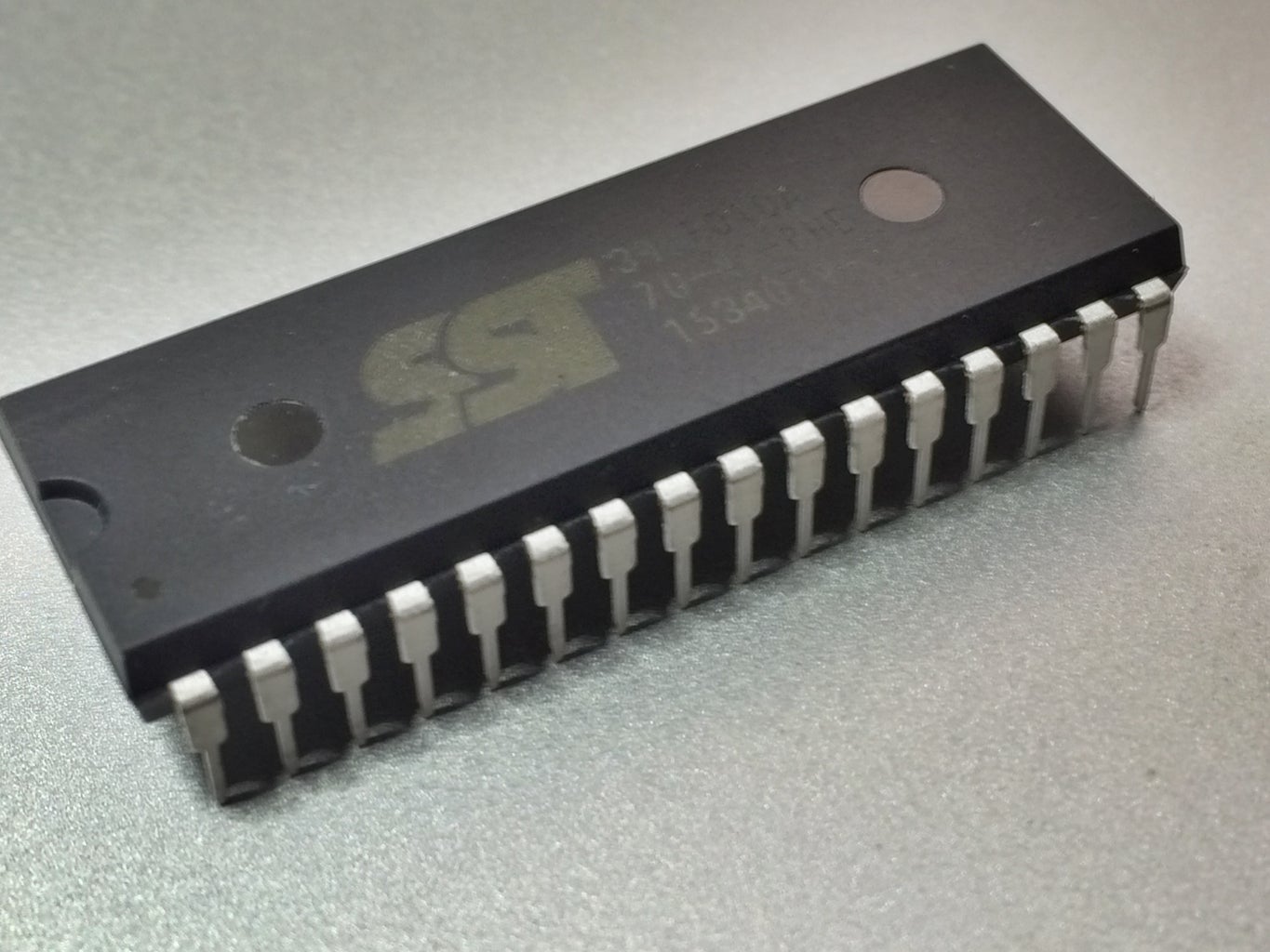


Battery profiler - my recent Arduino project - needed to store large amounts of data in some kind of flash memory controlled by Arduino. In the past, for this I used serial (SPI) chip W25Q80BV from Winbond that came in a breadboard-friendly PDIP-8 package. See this excellent tutorial on how this was done and reasons why this might be preferred from an SD card. The chip is no longer available, though, and while looking for alternatives I flirted for a time with parallel flash memory. Parallel memory? At first, this seems like a hopeless mismatch with Arduino. Parallel logic chips, after all, feature a lot of pins that need to be connected, well, in parallel. For example, the chip I used, SST39SF010A, has 32 (!) PDIP pins. Address pins alone count to 17! There is no way pin-poor Arduino, such as Pro Mini, could handle this kind of load. However, with a few additional chips I could successfully serialize the memory chip using as little as 6 Arduino pins plus I2C pins for communication.
In the end, I overcame my fear of surface mounted components (soldering these is actually easy!) and my finished battery profiler uses a tiny in size, but powerful 32 MB modern _serial_ chip from Winbond in SOIC package. But since I've spent quite an effort to connect the parallel memory to Arduino, write software, and get everything working, I decided to write this Instructable. Perhaps, someone will find it useful as a generic recipe of connecting parallel logic devices to Arduino. Maybe data recovery from a mobile device that died?
Step 1: Hardware

Parts:
1x MICROCHIP SST39SF010A-70-4C-PHE Flash Memory from Element 14
1x MCP23008 I/O Expander from Adafruit
2x 74HC595 Shift Register from Adafruit
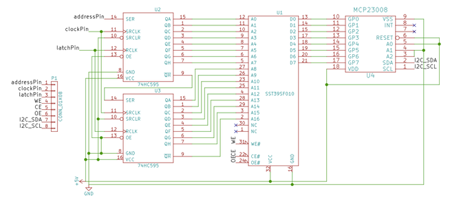
The SST chip uses pins A0 through A16 for the 17-bit address to cover its 128 kB of capacity. The 74HC595 shift register was designed to "convert" a single-pin serial input, pin SER, into 8-bit parallel output on pins QA through QH. Since the chip must "know" when one bit ends and another begins, it must use two additional pins for control (clock and latch). The beauty of this chip, however, is an additional output pin QH' that can be connected to the SER pin of another shift register effectively putting the two in a daisy chain. Two daisy-chained 74HC595's output 16 bits, three 24, etc. You get the idea.
To cover address space of SST39SF010A we need two shift registers. "Wait a minute", you may think, "this does not add up. How 16 parallel pins can connect to 17 needed by SST39SF010A?" Ah, my friend, the QH' pin of the last 74HC595 in the chain provides the missing 17th bit. Thus, there is no need to "waste" a third shift register just to cover one bit. See the attached schematics: two shift registers nicely cover all the memory address pins A0-A16. Overall, shift registers use 3 Arduino pins.
As nice as the 74HC595 is, it can only send parallel bits, but does not receive them. Hence, to connect the SST's data pins, D0 through D7, to Arduino we need another solution. It presents itself in the form of the MCP23008 I/O expander from Microchip. It's more expensive than shift registers, but it can read 8 bits in parallel and shift them to Arduino via the I2C protocol on pins SDA and SCL. The corresponding pins for I2C are A4 and A5 in Arduino Pro Mini (in the middle of the board) and pins 20,21 in Arduino Mega. These are the only 2 Arduino pins the chip uses, which is not a big deal considering that multiple I2C devices can be connected on the same line. The obvious question is: can one use three I/O extenders instead of two shift registers for SST's address pins? Yes, of course. Be my guest and make that modification.
The last connections must be made to the WE#, CE#, and OE# pins on the memory chip itself: these are used for chip control. Thus, the total use of Arduino pins counts 6 digital pins plus 2 I2C pins.

Step 2: Software
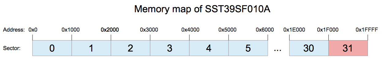

Ptorelli has already described how flash memory works saving me a ton of writing. The SST chip is no different: blank chip fresh from the factory has every bit set to "1" or, if you prefer, every byte reads 0xFF in hexadecimal. Ptorelli explains why you can easily write to a single byte, while erasing has to be done one sector at at time, at minimum. The The SST's sector size is equal to 4096 bytes (0x1000 in hexadecimal) and SST has 32 sectors in total; see the above image. Ptorelli also explains why flash memory has a finite lifetime of 100k erasure cycles. If data storage starts from byte 0, for example, every time, then the first sector would "die" pretty quickly, while last sectors would remain unused. Therefore, data storage has to be planned carefully with some kind of wear leveling. I have adopted the simplest log-structured algorithm of wear leveling. In my case I reserved sectors 0-30 as a circular buffer for storing the data, which is written sequentially from byte 0x0 to byte 0X1EFFF, then wrapped around back to 0x0. The last sector, number 31, serves as a circular buffer for storing 3-byte addresses of the start of each file. In my application I only care about the last written chunk of data, but you are welcome to build an actual file system by, e.g., adding names and/or dates.
The libraries I wrote for this project are available from these repositories:
https://github.com/aromring/Adafruit_MCP23008_RF
https://github.com/aromring/ParallelMemoryInArduin...
The ParallelMemoryInArduino library also contains a demo sketch that:
1) reads lastly written 20x4 table of floats from the chip and displays it in the Serial Monitor
2) writes a new 20x4 table of random floats into the chip
One of the above images contains typical output.
