

Introduction: Intro to Printed Circuit Boards


In this instructable, I'll go over what a printed circuit board is, where they are used, and the basics of how to make one yourself. So sit back, strap in, and enjoy learning about this very important and interesting method of making electronics!
Note: this is an introductory guide. I'm sure that there is a lot I did not cover, and if you find something you think I should mention in this guide, make sure to put it in a comment below!
Step 1: Creating Circuits


When creating a circuit, you need to connect multiple electronic components together, usually to perform some useful function. There are many different ways to do this:
- Breadboard
- A common method of prototyping circuits.
- Pros
- Great for building temporary circuits and some quick projects.
- Quick and Easy
- Cons
- Very impermanent; wires and components can easily be pulled off
- Restricted to through-hole components
- Point to point
- (solder components directly to each other)
- Pros
- Don't need a board for your projects
- Quick construction
- Can take up less space
- Cons
- Not very organized
- Hard with small components
- Difficult to repair
- Wire Wrap
- Use board of pins and wrapped wires for connections
- Pros
- Fast if you have the tools and materials and a simple circuit
- Cons
- Can be very disorganized
- Difficult to repair
- Proto-board
- Plated or non-plated holes in fiberglass for circuit construction
- Pros
- More organized than point to point
- Can be easily mounted in a case
- Can have relatively quick construction
- Cons
- Labor intensive to make circuits
- Conductive Ink
- Ink with a very low resistance that can be painted on and used as a circuit
- Pros
- A cool, novel way of making circuits
- Good to get kids interested in making simple circuits
- Cons
- Not very practical
- Cracks easily
- Low conductivity
- Conductive Thread
- Similar to conductive ink: cool and novel, not too practical in most cases. However, some cool uses in wearables!
And finally, Circuit Boards!
Step 2: What Is a Printed Circuit Board

A Printed Circuit Board (or PCB for short) is a different way of connecting electrical components together. It is made out of a non-conductive material, usually fiberglass. However, there is a layer or multiple layers of copper over the board, which lets you connect components when the copper is etched away in the correct patterns.
The board in the image above was made with a CNC machine which mechanically removed a copper layer in specific places to allow components to be soldered on and through the board, and be connected together in the right way. While this one isn't, many are then coated with a solder mask of a certain color, often green (but not always) that helps solder stick to the right places.
PCBs are great for creating circuits because they are:
- Inexpensive
- Can be mass produced
- Reliable
- Are the industry standard
PCBs are in almost everything electronic; computers, mice, electric scooters, refrigerators, screens, phones, and countless other devices.
The world market for printed circuit boards (PCBs) reached an estimated $60.2 billion in value in 2014, and is only growing larger: http://www.iconnect007.com/index.php/article/9297...
Step 3: Designing a PCB

The first step to designing a PCB is knowing what you want to make. There can be a lot to designing a PCB, or it can be extremely simple; it completely depends on what circuit you're making.
But whatever you end up making, it's helpful to have a program to organize it all for you and give you the tools you need to turn a schematic (abstract diagram of all the parts and connections you need) to a final layout for your circuit board. From there, you export your file and can send it off to be fabricated.
Some programs for PCB Design:
- Altium
- KiCad (free)
- CadSoft Eagle
All these programs are designed to do the same thing; help you make your PCB. Some things you will need to create:
A board shape to define how large and what shape your board is
Component placement: where are your parts?
Trace routing: these connect all your components
File Export: export industry standard gerber files for manufacture
There's also lots of other circuit components your board could have, some of which I'll briefly list here to help spur your imagination:
- Vias: connect traces to multiple layers of copper
- Through holes: for parts with leads
- Surface mount pads: to connect surface mounts parts
- Ground/Power planes
- Test points
- Holes/slots
- Integrated antenna
- Multiple layers
Step 4: Want to Make a PCB?

So you want to make a PCB? Well good, there's tons of different methods you can use.
Fab House
Probably the most effective and easiest way is to send your gerber files to a fab house. These take the files you created in your circuit creation program and fabricate a board for you. I'll go over these a bit more in the next step.
CNC Machine
You can also use a CNC machine to create your board if you have access to one. I've personally used a machine at work made by LPKF, which is specifically designed for making circuit boards and the Othermill by Other Machine Co. The Othermill is designed for hobby grade CNCing, and can carve out 3d shapes into blocks of soft material or mill away a double-sided copper clad board to create a PCB.
Chemical Etching
Finally, the cheapest of the three; etching your own board at home with multiple stages of chemicals to eat away the areas inbetween the traces. I'll leave it an exercise to the viewer to find out how this interesting process works: https://www.instructables.com/howto/etch+PCB/
Step 5: Getting PCBs Made

A popular option for getting PCBs is to have them made by a fab house. These are professional facilities that handle construction of possibly thousands of boards a day. Each fab house is of varying quality and has different tolerances of trace width, hole size, and other specificities like cutting slots so you should do your research before sending your files out anywhere.
Some places will have discounted shipping but longer lead times, or only offer smaller batches so are good for prototypes but not when you need a lot of boards. Everyone has their preference for places and it's up to you to choose which place to use. Here are a few:
- Alberta Printed Circuits (APCircuits.com)
Advanced Circuits/4pcb.com/Barebones PCB/33Each.com/FreeDFM.com
E-TekNet
Gold Phoenix
Olimex
OurPCB
PCB123/PCB Express
Sierra Proto
PCBCart
And due to popular demand: http://pcbshopper.com/
PCB Shopper lets you compare multiple different fab houses and determine what place is right for your needs.
More info: http://www.ladyada.net/library/pcb/manufacturers.h...
(note: old article)
Image: https://www.element14.com/community/servlet/JiveSe...
Step 6: Adding Components

Once you have your bare PCB, the next step is adding your components. These need to be soldered on, but there's more methods than just doing everything by hand.
By Hand
I know I said there's other methods, but as long as you don't have huge components and a steady soldering iron, placing components by hand is still a great way to go as long as you don't have dozens or hundreds of boards to solder. So get those tweezers out!
Pick and Place
Pick and place machines automatically grab components and put them onto the right spot on the board. These are really cool machines! You should look up a video of them in use, it saves tons of time in assembling electrical assemblies. However, these are very expensive! Your fab house might offer to do placement if they are adding components, in which case they might use this machine for large quantities of the same board.
Reflow Ovens
Reflow ovens can be used with either pick and place machines or placing by hand but are generally for surface mount parts. Solder paste is first applied before component placement. Then, the PCB is placed in the oven, and temperature increased and then brought down again at a precise interval. This is hot enough to melt and reflow the solder paste, securing all components to their pads, but not too hot to damage any components.
Wave Soldering
This has been somewhat replaced by reflow ovens due to increased popularity of surfac mount components, but is still an effective method. Heated solder is pumped up in a wave shape, and boards passed into the wave to quickly solder multiple components to a PCB.
Step 7: Non-traditional PCBs


There's also some different and pretty cool types of PCBs.
Flexible: These boards can bend and twist. While not used very much, they can be useful when a device needs to be small and light, such as in wearables.
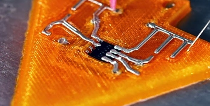
3d-printed (Voxel8): At least one company now is making a 3d printer that can integrate conductive traces with printed plastic layers. This way, electronics can be integrated with mechanical parts; all in three dimensions.
These technologies are not too popular at the moment, but could possibly be used more and more if price comes down. Make sure to keep an eye out for future flexible and 3d printed products!
Thanks for reading my instructable, and I hope that you learned something new about PCBs!
Flexible PCB Image: http://www.businesskorea.co.kr/sites/default/files...
3D printed circuit image: http://www.technocrazed.com/wp-content/uploads/201...

Participated in the
Makerspace Contest


