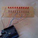
Introduction: Learn Verilog: a Brief Tutorial Series on Digital Electronics Design With FPGAs and Verilog HDL


This brief series of semi-short lessons on Verilog is meant as an introduction to the language and to hopefully encourage readers to look further into FPGA design.
These tutorials assume you are familiar with basic logic circuits and logic equations, as well as associated behaviors.
I pose this question to you: If F = (A • B), and A is logic high and B is logic low, what is F? If you cannot answer this question, I recommend you re-visit your logic circuit studies. Logic circuit tutorials are a possibility if enough requests are made.
Checklist of basic things to know before you begin:
- The functions of basic logic gates (AND, OR, NAND, XOR,...)
- The difference between "logic high" and "logic low" and which one is represented by a "1" and which one by a "0"
Familiarity with C/C++ is helpful (at times) but not required at all.
If you are prepared to follow along with this tutorial, you will need two things:
- An IDE for your Verilog (I highly recommend Xilinx ISE Design Suite; after registering for free you may download this very robust IDE)
- A FPGA digital design board (I prefer Digilent Inc.'s boards for their ease of use and "hard to ruin" design)
There is ample documentation on the ISE out there so I will not be going over how to use the software.
The picture on this Introduction is of a typical ISE window with text editor, module directory, and process pane open.
Oh, and on some slide you'll see titles that start with VM x.x; this stands for Verilog Module and makes it a bit easier to keep track of.
On to Verilog!
Step 1: VM 1.0: Verilog Background

What is Verilog, anyways? The short answer is: a hardware description language.
But without any context or further definition, that's all Verilog will mean to you. Hardware description languages (in the context of Electrical Engineering) are used to formally describe the behavior of a circuit. This should not come as a surprise given the not very creative title of "hardware description language" (which is often more simply referred to as HDL). Several HDLs exist, but perhaps the two most common languages encountered are Verilog and VHDL (You may be tempted to shorten "Verilog HDL" to VHDL, but these are two distinctly different languages, so just call it Verilog!).
We can use HDLs such as Verilog for many things; it's most important use, however, is to unambiguously describe a particular circuit. This includes describing its inputs, outputs, and behavior. When used in conjunction with a Field Programmable Gate Array (or, FPGA) board, we can create an infinite number of circuits just by changing its description in Verilog; a powerful prototyping tool. We can also use Verilog without a physical device to simulate circuits and run "testbenches" on our HDL to see how the circuit would behave should we actually build it (i.e. Did the circuit behave like we wanted?).
Pictured: A portion of Verilog that describes a state machine. This short primer won't come anywhere close to that complex code!
Step 2: FPGA Overview and UCF Files

Before the dawn of FPGA boards such as the Digilent Basys 2, prototyping a digital circuit meant purchasing each individual component of the circuit (including gates, structural blocks such as multiplexers, and so on) and hand connecting all the parts, often with a breadboard and jumper wires. Using Verilog, an FPGA chip, and built in stimuli on the board (e.g. LEDs, switches, buttons) we can easily create circuits and see the results in comparably little time. How does this work?
An FPGA chip acts as a blank slate for your digital circuit; IDEs (Integrated Development Environments) such as Xilinx ISE Design Suite can transform your "high level" Verilog into bitstreams that tell the FPGA what to implement. So instead of buying a multiplexer (also known as a mux), switches, and LEDs, we can describe in Verilog a mux that has inputs and output(s), and also in Verilog tell the FPGA where on the design board the inputs are coming from and where we want the output(s) to go. We accomplish the creation of a full circuit in two parts: Verilog modular code and a User Constraint File (UCF).
As you may have guessed, the Verilog code (which we create in chunks called "modules") describes what should happen in the circuit, and the User Constraint File tells the FPGA chip what each of its pins does in the circuit; the FPGA chip has a number of pins that can serve as inputs and outputs and to complete our quest to unambiguously describe the circuit we have to declare what ones we will be using. For example, say pin G12 on your design board is physically connected to an LED, and in your Verilog code you will eventually have a circuit driving that LED. If in your Verilog you refer to that LED with the uncreative name "LED", you must (before any bitstream is generated) tell the FPGA by way of a UCF file that "If I say LED anywhere in my code, you should actually refer to pin G12." This allows the engineer to have "nice" and meaningful names for components found in the circuit while still being able to generate low-level code. Of course this is not exactly how we would put that statement in a UCF, nor is this the only thing you can specify in a UCF, but we will dive into UCFs in another module.
One last note on UCFs: Different digital design board manufacturers will use different pin locations for different components; each model is unique. Typically, you can get a "Master" UCF from the board manufacturer that contains all possible stimuli, and you can reuse this file in your projects by commenting out constraints that do not apply and by changing names as you see fit. Beginners should not modify any other attributes of the UCF other than names; doing so without having advanced knowledge may cause board damage or other "interesting" and undesired outcomes!
Pictured here from Wikipedia is an FPGA chip manufactured by Xilinx, one of the world's top FPGA manufacturers. This chip will implement the circuit you describe using Verilog.
Step 3: VM 2.0: Your First Verilog Project

Note: I said "project" not "code". Despite the fact that we develop FPGA designs using what resembles a programming language, the outcome is not a program; all of your hard work yields an actual circuit.
Even though you are barely exposed to Verilog, I feel you'll learn best by jumping right into the HDL pool. Don't worry though, we'll walk through all the code together, and I'll be sure to explain why and how things work. I learned the hard way that Verilog builds upon itself very quickly, so it behooves you to get a solid foundation of understanding.
Note: Despite how convenient it is to copy and paste code, I highly recommend you re-type everything so that you understand it better. Try it; it works.
Before we begin, I want you to pay special attention to the following traits of my code:
• Case sensitivity: Verilog is case sensitive! Keywords must be typed with proper casing (lowercase) and any user named inputs, outputs, or other pieces of code must always be referred to as they were first declared.
• Indentation: Although not as apparent in this example, indentation is a big deal in Verilog (as with many other programming languages). While the compiler and software suite will work with poorly formatted code, it is poor style to not observe indentation rules (which will be explained later).
So without further ado, here is, in my opinion, the "Hello, World" equivalent in Verilog:
----------------------------------------------------
`timescale 1ns / ps
//this is a comment in Verilog
module hello_world(
input switch[0],
input switch[1],
output led
);
assign led = switch[0] & ~switch[1];
endmodule
------------------------------------------------------
Now, this is not the most efficient implementation of the module. Let's start looking at the code piece by piece and see if you can find out how you could improve it.
Step 4: The "Timescale"

`timescale 1ns / ps
This code is a compiler directive that sets the "reference time" (in this case, 1ns) and the "precision time" (in this case, 1ps). In circuits you will actually implement on your design board, timescale is not that important as the FPGA cannot implement specific gate delays or other manipulations of time. But for simulations this line is very important.
Later you'll find out that we can simulate gate delays to find glitches or have the system "wait" a set amount of time before it changes conditions. The "reference time" is what you can think of as the default unit: if you were to code a time delay (this will be explained in a later module) of "#5" the compiler will default to 5 nanoseconds. For simulation purposes, the most precise you can be is dictated by the "precision time," in this case, picosecond resolution.
Step 5: Comments in Verilog

//this is a comment in Verilog
Much like in C++ (you'll see that Verilog has syntax that is somewhat similar to C/C++) a comment in Verilog is denoted by "//". Anything after the double slashes on that line is ignored by the compiler. Comments are amazingly helpful during debugging and makes your code more understood by others. Multi-line comments can be done by using "/*" to open the comment block and "*/" to close it.
Don't be stingy with comments, but don't be excessive; and whatever you comment, make sure to keep comments current! If you plan on having stale comments you may as well not comment at all!
Step 6: The Module Declaration

module hello_world(
input switch[0],
input switch[1],
output led
);
module is a Verilog keyword. Think of it like a type declaration; in C++ we could have a function declaration of "void hello_world(<parameters in here>)". Notice the similarities?
While Verilog doesn't return any value (like a "void" C++ function), and is really not even a function, its syntax is similar and we can still think of module as a type declaration, and "hello_world" as the name (names in Verilog cannot contain spaces). Good Verilog code is "modular", and we'll discuss what that means later (further tutorials will soon be available on my personal website and possibly Instructables).
Inside the parentheses of the declaration are what we can equate as our parameter list. That is, the module HAS an input called switch[0], another input called switch[1], and an output called led. input and output are essentially variable types. There are a few quirks to module declarations that we'll look at in the next module.
Do you see how we could reduce our input and output declarations from three statements to two?
Hint: You can create arrays (called buses) in Verilog!
After all inputs and outputs are declared, the parameter list is closed with a matching parenthesis and a semicolon. The semicolon, much like in C++, marks the "end" of a statement. One convenience of Verilog is being able to split up large statements such as long logic statements into multiple lines for easier reading, as long as you don't forget the semicolon.
The picture shows the typical color coding of a module's declaration.
Step 7: Logic in Verilog

assign led = switch[0] & ~switch[1];
This line is where the "magic" happens. Up to this point, your code has described all inputs and outputs, and now you will manipulate outputs based on those inputs. assign is another Verilog keyword; one you will use over and over again. Assign statements are permanent descriptions of an output based on one or more inputs. You may not have more than one assign statement per output, but you can have more than just one simple logic expression per assignment. The closest C++ equivalent to an assign is setting a variable equal to a value, only in Verilog you cannot change the "value" after it's been set because after being set, the value depends on the physical states of inputs.
Remember, Verilog is a hardware description language, meaning you are only describing how a circuit behaves. The states of switch[0] and switch[1] may change while the circuit is live (e.g. You flip switch[0] to logic low voltage) but the assignment statement is resolute; led will only be driven to logic high voltage at "switch[0] & ~switch[1]".
So what about "switch[0] & ~switch[1]"? We know both are inputs, but what do the '&' and ' ~ ' mean?
When we handwrite logic equations for digital circuits, we use a '•' for AND, '+' for OR, ⊕ for XOR, and if we want to indicate the inverse, or "not" of a term, we draw a bar over it. There are equivalents to all these and more in Verilog, as seen in the attached table.
We can group together statements using parentheses; this is especially useful for creating NAND,NOR, and XNOR gates, as we implement the equation as we would for non-inverted version of the gate, add parentheses around the equation, and add a ' ~ ' to its front. For example, to make the Verilog statement of "F equals A xnor B", where would we start? Surely we need to "assign" F a value, so coding "assign F = " would be a good start... Ok, so A xnor B... We don't have an xnor symbol! No worries, we can make A XOR B then invert the entire term! This leads to a final solution of "assign F = ~(A ^ B);"
Note the operator precedence; the "INV" operator is associated with the term to its left, and the AND, OR, XOR, etc. follow standard logic equation precedence rules.
Don't forget the semicolon after the assign statement!
So going back to our example, assign led = switch[0] & ~switch[1]; means that led will be driven to logic high voltage if and only if switch[0] is a logic "one" and switch[1] is a logic "zero".
Step 8: Ending Your Verilog Module

endmodule
This line of code might seem out of place at first. How can we "end the module" without explicitly beginning it? In Verilog, we only define one module per file! Each module may contain instances of other modules, but they may not define them.
This keyword marks the end of the module (as I hope you could have guessed) and lets the compiler know that all the "useful" information is above that point. Sometimes, IDEs can be particularly fickle about endmodule placement, but if you ensure that there is a blank line before AND after the endmodule command, and that the endmodule code is not indented at all, you should avoid most issues.
Step 9: Preparing to Program Your FPGA Board
That's all to this module, so you are ready to put this onto your FPGA board! JUST KIDDING, what are we forgetting?
That's right, the UCF.
While, like mentioned before, each digital design board manufacturer has different constraints for different boards. A sample constraint is as follows:
NET "led" LOC = "M5" ;
NET precedes every statement, followed by the name of the net (in quotations), and then the actual LOCation constraint (also in quotation marks). The name can be set to whatever the engineer desires (although the best names are those that convey the most meaning in the least amount of space) and the location constraint indicates where the "net" is physically connected to the FPGA. A comment in a UCF is indicated differently than in the Verilog module; in a UCF, use a '#' to denote a comment. Some IDEs have built in features that allow you to batch comment code out by highlighting the desired code and pressing either a hotkey combination or button in the IDE.
So if you were to go through and create a UCF file for your board that contains a constraint for each input and output, your IDE would be able to create a bitstream for your FPGA board, in conjunction with the Verilog module you created earlier.
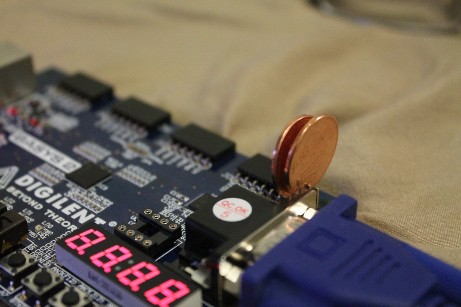
The process for programming different FPGA boards varies, so refer to your board manufacturer for specific instructions. The photo included is of my FPGA board plus my two cent pin jumper replacement (temporary, and I don't recommend you do this unless you absolutely must continue debugging like I had to).
Side note: Verilog modules are stored in files with a .v extension, and UCF files in a .ucf format. Both files are editable using Notepad or any other text editor (Wordpad tends to respect indentation rules better than Notepad).
Step 10: Reflection

Did your first program work!? If it didn't, try to figure out why. If it did, consider messing around with other operators in the assign statement: can you make led a logic 1 if switch[0] is a logic 0 OR switch[1] is a logic 1?
Pictured is what the "Processes" panel will look like in ISE should your Verilog and UCF create a valid bitstream. This doesn't guarantee that the circuit behaves how you want, just that acircuit will be created on your FPGA board.
Step 11: VM 2.0: Verilog Port and Wire Types

In the last example, you saw the following module declaration:
module hello_world(
input switch[0],
input switch[1],
output led
);
What do input and output mean in this context? These are identifiers that tell the compiler what kind of "port" you are creating. In Verilog we will deal with the following identifiers in the module declaration:
input : An input port, type "wire" is assumed. An input port may not be assigned any value within the module.
output : An output port, type "wire" is assumed. An output wire may be assigned a value using an assign statement, or have its value determined indirectly by an instance of another module. An output wire may not explicitly be assigned a value in any conditional logic (e.g. "if" statements).
output reg : An output port of type "reg", short for "register". This type of port can be given a value independent of other parts of the circuit (e.g. assign it a logic "1") and keep that value until changed. If you will be changing the value of a port from within an "always" block (a chunk of code that executes at any change of its parameters) you need to use a reg.
In short, a wire serves as a connector form one point to another, like from a real word source to an AND gate, and a reg can create its own source that goes to some destination.
Inside of a module we can create internal wires and regs for use inside the module. This is useful when you need to make the input of one instance of a module equal to the output of some other instantiated module. Since a wire doesn't have its own driver you can make its source the output of one module, and its destination the input of another. With this in mind, how do you think you would declare a wire or reg for use inside of a module?
wire my_wire;
reg my_reg;
Note that we don't have to specify if the wire/reg is an input or output for internal wires and regs because in order for it to properly route in our design we will eventually give it a source and destination.
In Verilog we can assign an output wire equal to an internal reg or wire. This lets us change the value of an output conditionally since if we change the reg we are also changing the output (remember that directly changing the value on an output is prohibited).
Applicable to all of the aforementioned ports, wires, and regs are what we call busses, or, vectors (arrays). We can group together similar signals using a bus. In the last example I posed the question of "Is there a way to only define 2 ports for three total inputs and outputs?" Using a bus we can. Instead of declaring "input switch0, input switch1" we can simply declare "input [1:0] switch". This creates a two bit bus called "switch". We can refer to specific parts of "switch" by using the [] operator as in "switch[0]". Busses are very useful in Verilog as it reduces the amount of code we have to produce.
Declare a bus using the following syntax ("type" refers to input, output, wire, or reg):
<type> [<max index> : <min index>] <bus name>
If you are declaring a bus inside of a module, be sure to add a semicolon at the end. If you are declaring a bus in the module declaration be sure to comma delimit all your definitions.
What implications does a bus have on your UCF file? All components of the bus will be given a name that begins with the common name and is followed by its index in the bus. So "[1:0] switch" will go into the UCF as two entries, "switch<0>" and "switch<1>". Remember to use the <> operators for the UCF!
Pictured are breadboard jumper wires; you won't need to worry about those on most FPGA design boards as they will have built in stimuli such as switches.
Step 12: VM 3.0: Modular Design

Please pay close attention to modular design. This is perhaps the single greatest topic in Verilog and is also perhaps its most powerful and useful feature.
By now you should be able to implement simple logic functions using basic Verilog operators ( | , &, ...) and get it to successfully run on your FPGA board. If you're not quite to that stage, please start with VM 2.0.
In "VM 2.0: My First Verilog Project", I introduced the concept of "modules" and "modular" code; now there are a few nuances of modules you need to know in order to be a proficient "modular designer". But first we need to discuss "What is Modular Design?"
If you completed the "hello_world" exercise, you were introduced to the Verilog keyword "module". Each Verilog source file contains one and only one module definition. So how can we create complex projects that involve many smaller modules? Let's take the example of building a timer controlled LED circuit. What would we need in our circuit to make an LED blink every second if some switch was a logic one AND we only had a 50MHz clock?
Break down what we need into three types: inputs, outputs, and internal components.
Inputs: Physical signal sources such as an oscillator ("clock"), switches, buttons, data ports, etc...
Outputs: Physical outputs that will be driven by the circuit like LEDs, data ports, displays, etc...
Internal components: Components that take the state of the inputs to generate a desired output; not all of these have to be connected to "top level" ports, but eventually everything should "route".
Read these classifications again; it is vitally important you know the differences! Also, note the new vocabulary words: "top level" and "route".
Think about what these terms might mean... I'll formally define them in a minute.
Liken these three types of components to an algebraic equation, the inputs are the independent variables, the outputs are the dependent variables, and the internal components represent the actual equation. Remembering this analogy will help you decide when working on projects if a given component is an input, output, or internal component.
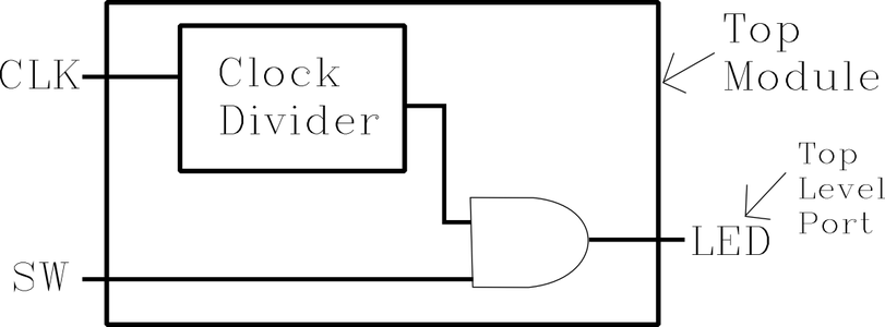
In the case of the LED blink circuit, here is what we have on a very high level:
Inputs: 50MHz clock, switch
Outputs: LED
Internals: A 50MHz to 1Hz clock divider, one AND gate (because LED should only come on if both the divided clock AND the switch are logic one)
How would you, on a very high level (meaning mostly "black boxes" to represent components rather than gate patterns), block diagram this circuit? Recall that you can make a clock divider by connecting a number of D-Flip Flops (DFFs) together along with some inverters.
See the attached diagram for the answer.
Challenge: In reality we would have a physical button that would reset all the DFFs in the clock divider. Can you draw the origin and destination of a button called "RST" on this block diagram?
Block diagrams like this are the first step to helping you figure out how to write a Verilog program, as every box in the diagram will end up as an instance of a module in your code. Notice that we have one large block that contains a number of smaller blocks; we call this the "top" module. The "top" module is what takes care of connecting all the internal components of the circuit to physical inputs and outputs.
Inside this particular top module are two things: a clock divider and an AND gate. But notice the clock divider block also contains a number of smaller blocks (DFFs). We DO NOT have to create all these DFFs in our top module; we can create a separate clock divider module that contains all the DFFs and create an instance of that clock divider in our top module.
As you could have guessed, we also need to make a DFF module which we can instantiate a number of times in the clock divider. This allows us to only define the behavior of a D-Flip Flop ONCE, then instantiate multiple instances of that DFF. All we have to do in our Verilog code is connect each instance of the DFF to the appropriate ports (i.e. connect its inputs and outputs), but more on module instantiation later.
Note: Don't try to code this blinking LED project just yet; there are a few more things we need to cover.
The point of this module is to expose you to modular design; do you see why I call these tutorials "modules"? This idea should be ingrained into your mind as you continue learning and using Verilog.
Step 13: VM 3.1: the Top Module
The top module in a Verilog project represents the highest level of your project. If you were to make a complex circuit, say, a stopwatch, which was internally composed of several less intricate components, the top module would represent what the user would see in the end: a "box" that shows a time, and has start, stop, and reset buttons.
But in that top module, unseen by the user, are a number of other modules such as counters, comparators, flip flops, etc. that are used by the circuit, but not necessarily connected to top level ports.
Top Level Ports: The absolute beginning and end of a project; real-world physical signal sources and destinations
The top module is responsible for properly connecting all of its instantiated modules to sources and destinations located within the top level, but does not define any of the behaviors exhibited by the instantiated modules. Remember, only one module can be defined per file!
Sometimes the top module is referred to as a "wrapper" because it "wraps" together all other modules in the project.
Next we will examine how module instantiation works.
Step 14: VM 3.2: Instantiated Modules
We've discussed instantiated modules a lot by now, so it's time to understand the underlying concept.
The top module wraps the project together, often by instantiating other useful modular components to meet project requirements. But each of these instantiated modules can ALSO instantiate other modules.
This means that a given top module can instantiate something like a clock divider, and that clock divider can instantiate a number of DFFs, but the task of connecting DFFs together is given to the clock divider module.
Sound like a familiar concept? Anyone who has dabbled with programming in languages like C, C++, Java, etc. should be familiar with "scope". The scope of an instantiated module is limited to the module that instantiated it. This is VERY similar to, for example, C++. If we were making a C++ program, we have a main() function that wraps everything together, and in that main function we can call other functions, but the internal workings of those functions (and those functions can also call these functions) are not accessible in main, even though to execute the main function, all the auxiliary functions must also be executed.
So in the case of the clock divider, the top module contains a clock divider, and therefore also contains a bunch of DFFs, but as far as the top module is concerned it doesn't have accessible DFFs.
Step 15: VM 3.3: How to Instantiate a Module
In the previous module I mentioned similarities between instantiating modules in Verilog and calling functions in C/C++.
Let's look at how we would instantiate a module in Verilog.
Here is the module we'll be working with:
`timescale 1ns / 1ps
module srlatch(
input S,
input R,
output Q
);
wire Q_int, Qn_int;
assign Q_int = ~(S & Qn_int);
assign Qn_int = ~(R & Q_int);
assign Q = Q_int;
endmodule
By now there shouldn't be any Verilog in this module you couldn't explain.
So let's say we wanted to make a circuit with two SR-Latches (regardless of how nonsensical this circuit is in reality), each with a switch for their "set" operation and a shared reset button. The output of each latch will be an LED.
With these specs in mind, let's make the top module's definition. Remember, top module declarations will only contain inputs and outputs that come and go from the real world.
`timescale 1ns / 1ps
//Challenge: Re-write this module declaration using buses
module top(
input switch0,
input switch1,
input btn0,
output led0,
output led1
);
endmodule
Great! Now we need to add two SR-Latches to our circuit. How would we do this?
Don't say "Hard code the behavior of two SR-Latches and assign their inputs and outputs respectively." We will instantiate two instances of an SR-Latch. Here's how our top module will look after the instantiation:
`timescale 1ns / 1ps
module top(
input switch0,
input switch1,
input btn0,
output led0,
output led1
);
srlatch sr0(
.S(switch0),
.R(btn0),
.Q(led0)
);
srlatch sr1(
.S(switch1),
.R(btn0),
.Q(led1)
);
endmodule
So what is left to do? Nothing; absolutely nothing (assuming you already have a UCF file ready). Why?
The reason lies in the module instantiation. Let's take a closer look at one.
srlatch sr0(
.S(switch0),
.R(btn0),
.Q(led0)
);
First line: srlatch sr0(
This is a very important line whose form you need to commit to memory. First comes srlatch. This is the name of the base module we are instantiating. sr0 is the instance name. The parenthesis opens the instantiation. Every instantiation will begin like that; "<module to be instantiated> <instance name>(".
There are some less common cases where instantiation will slightly differ, but even then this form will still be present.
The next three lines:
.S(switch0),
.R(btn0),
.Q(led0)
Take a look at the srlatch module port names and then look back at these three lines. This is, in a roundabout way, similar to how we call a function in C/C++; this is where we pass the parameters.
The difference is that in Verilog we are passing both inputs to the module AND outputs to the module. That is, we are telling that specific instance of the module where its inputs are coming from and where we want the outputs to go.
Another way to look at this is that we are passing the module a set of inputs and outputs, each whose value is continuously updated either from inside the module (outputs) or outside the module (inputs).
Let's break down the statement: .S(switch0)
Every module instantiation will have a series of statements similar to this one, one statement per input/output. The ".S" is referring to the input S in the srlatch module, and the (switch0) is referring to input switch0 located in the top module. See a pattern?
. <port name in instantiated module> ( <port name in current module> )
This concept is also similar to calling functions in other programming languages like C/C++; in the function call we pass values (that we know by variable name) into the function. We call this value one thing in, for example, main, but in the function it is called something different. In this Verilog example, we have an input in the top module called "swtich0", and we want the "S" value of "sr0" to be equal to whatever "switch0" is.
Like I mentioned before, you need one port initialization statement per port in the module you are instantiating, but if you are instantiating a module that has, say, a [7:0] bus input called "T", you don't need to make 8 statements like ".T[0](Input[0])". You can pass entire busses by referring to the names only, so you could pass "Input" into "T" by stating ".T(Input)". Keep in mind though that bus dimensions MUST match up (i.e. you cannot pass a 5 port bus into a module who has a 3 port bus).
Additionally, port types must match up. You can only pass an input to an input, and an output (or a wire; more on that later) to an output.
Separate port initialization statements with a single comma. Good coding style dictates that each line only contains one instantiation. From this you should be able to understand those three lines of code.
Close the instantiation with a matching parenthesis and a semicolon.
After the instantiation is successfully done, the outputs of the instantiated module will, in essence, be accessible within the current module. You can then route these outputs to top level ports or even the inputs of other instantiated modules.
Before we end this discussion, let's summarize how to initiate a module (remember that "current module" refers to the module that is doing the instantiation):
<module name> <name of instance> (
.<port name in module to be instantiated> ( <port/wire name in current module> ),
... <repeat above as many times as needed>...
.<port name in module to be instantiated> ( <port/wire name in current module> )
);
Step 16: VM 3.3: Advanced Instantiation Topics

(Image originally created by Digilent Inc.; modified by me for this this tutorial)
The previous module introduced, and hopefully drove home, the concept of instantiation in Verilog. Now we will take a look at a couple advanced topics (second topic to be added soon) regarding module instantiation.
Counter controlled instantiation:
What if we needed to generate a bunch (take 50 as an example) of DFFs that were all connected together in a clock divider circuit... We already know how to make a general DFF module, so now we need to instantiate it 50 times and connect the clock pin of each one to the output of the DFF that is sequentially before it, connect reset to a global reset, and the D in pin to the inverse of the DFF's output (Q). Use the attached diagram for reference.
This would be a lot of instantiations for you to write (50 instantiations times 6 lines per instantiation is 300 lines!) by hand. But in Verilog we can use a counter controller loop, specifically, a "for" loop, to instantiate (generate) all of these modules (except for the first one) for us in very few lines of code. But there is one caveat; we have to carefully plan our design so that we can use a "generate loop" properly.
Note that the way we connect each DFF to the next is uniform and predictable. Of course, the first DFF's clock will be the clock input from our top level module, and the output of the last DFF will go somewhere in the top level module, but we can deal with those individually; during the generation, each internal wire in the design except for the first clock that we will manually designate and the last output wire will be explicitly given a source and a drain. The software knows that the two remaining wires need either a source (first clock) or drain (last data) and it is the engineer's responsibility to provide one.
As mentioned before, you have to set up the design properly in order to use a generate loop. What does this involve? Well, it makes sense that since each DFF is going to have a clock in dependent on the previous one (not including the first one!) that we can group together these similar signals in a bus! This lets us refer to signal groups like an array in C/C++ and call individual wires by index using the [] operator.
The reset pin for each DFF will come from a common reset, since each DFF needs to be able to reset at the same time.
Without knowing the specifics of a generate loop yet, we can still make our bus that will be used in the design. What type of bus will we make? Since these are only carrying a signal from a source to a drain, we will make wires.
wire out[49:0] //50 bit wide bus for DFF output/input
We can also instantiate our first DFF. Using the DFF module from Tutorial Module 3.2, and assuming our clock divider has an input clk (a clock pin), an input rst (a reset pin), and an output out (let's say it will drive an LED, creating a blinking effect).
dff dff0(
.clk(clk),
.rst(rst),
.D(~out[0]),
.Q(out[0])
);
Now, the generate loop. It is similar to a loop in C/C++ but has its own nuances. First we need to create a counter variable. In Verilog the variable type is called "genvar" and it is used to declare a variable, call it "y", like so:
genvar y;
The generate loop begins with the keyword "generate" and ends with "endgenerate".
Note: You must declare any genvar variables outside the scope of the generate loop.
We now have:
genvar y;
generate
endgenerate
Immediately following the "generate" keyword is the actual loop. Its declaration is like a loop in C/C++, but in Verilog, we don't have the luxury of left and right curly braces ( { and } ) but we do have the Verilog equivalent: begin and end. Additionally, Verilog does not support postfix operations, so we can't state "y++" and must instead state "y = y + 1". When constructing the for loop, keep in mind that we already created the first DFF (DFF0) so we will generate from 1 to 49 (smaller than 50).
genvar y;
generate
for(y = 1; y < 50; y = y + 1 ) //spaces may be omitted
begin
end
endgenerate
With a generate loop, we are going to "begin" an instantiation loop and must give this process a name. We will not use this name for any other purpose and will not refer to it later in our design (it is used internally in the synthesizer). We do this by adding a statement following the format " : " and place it on the same line as the "begin" for good style. Let's call this "dff_generation":
genvar y;
generate
for(y = 1; y < 50; y = y + 1 ) //spaces may be omitted
begin : dff_generation
end
endgenerate
Now is the crucial and most difficult part: creating the instantiation model. This will look just like any other instantiation except that the wires you pass the module are allowed to use the genvar as a value or value modifier. Recall that the genvar's value will change by one in this case after each instantiation.
Rather than walk through each line of the instantiation I'll give you the entire block of code and point out things you may not recognize. Be sure to refer to the provided picture to see how this circuit is implemented.
genvar y;
generate
for(y = 1; y < 50; y = y + 1 ) //spaces may be omitted
begin : dff_generation
//the below instance name doesn't matter
dff dff_insts (
.clk(out[y-1]), //clk in of DFF "y" is out of "y-1"
.rst(rst), //each DFF gets the same reset
.D(~out[y]), //input is fed the inverted output
.Q(out[y]) //output
);
end
endgenerate
I encourage you to hand trace a few iterations of the loop to see how the generation process works. The synthesizer will give each instance it creates a unique indexed name such as "dff_insts1" and "dff_insts2".
Step 17: VM 4.0: Introduction to Behavioral Verilog
Congratulations! You've made it this far and now is the time where your projects can get super complex with relative ease using "behavioral" Verilog.
So far we've been mostly discussing structural logic in Verilog. This means your circuit's behavior is set once using assign statements and logic statements using our logic operators, and when programmed on the board behaves as specified without taking into account what the inputs are (this isn't to say that the inputs don't affect the output, just that every possible combination of inputs is evaluated with the exact same logic). Behavioral logic allows you to change a circuit's behavior based on the state of given inputs.
The idea similar to this sort of Verilog code found in non-HDL programming languages such as C/C++ is seen in the form of control loops and if/else/case statements.
The rest of VM 4 will cover the basic types of behavioral Verilog and ways to implement it.
We will also discuss the difference between blocking and non-blocking statements; a very important but often overlooked concept. I once overheard a teaching assistant ask a student a question about the operating specs of his project in my Logic Circuits' lab, and when the student didn't have an answer to a question that was easily answered if he read through the assignment all the way before he started writing code, the TA responded with something like, "This is a big problem that so many engineers just write the code and don't know why they did what they did." This stuck in my head, and it dawned on me that I was only told when to use blocking and non-blocking statements but never told why or what the difference was, so this is a topic I feel is very important to discuss.
Step 18: VM 4.1: the Always Block
If someone mentions the words "Verilog" and "Behavioral" in the same sentence, your brain should hopefully immediately think "always block". There isn't a true translation between an always block and anything in a language like C/C++, but the concept is not hard to understand. But if you must have a comparison to C/C++, an always block is like a while loop who's condition of when to evaluate is a mess of if statements.
In a nutshell, an always block is a section of Verilog coded logic that is evaluated every time a trigger's condition changes.
What does this mean? Let's look at a basic always block for a circuit with two inputs, sw0 and sw1.
always @ (sw0, sw1)
begin
end
There is no body code to this block, but let's ignore that for now. Notice the '@' that proceeds "always" ("always" is a Verilog keyword). Also notice the statement inside of the parentheses: "sw0,sw1".
Using a simple truth table, we know that for two inputs there is a maximum of 4 unique states the inputs could be in: both logic high, both logic low, and one high one low for both inputs.
The "always @ (sw0,sw1)" essentially says "If at any point any input changes its state (i.e. change of row on the truth table) then re-evaluate the following code:".
This wouldn't be too simple to write in C/C++, but in Verilog it is that simple. An always block will re-evaluate the code within its scope (between the begin and end statements following the "always" declaration) when one of the listed triggers (that list is called a sensitivity list) changes either from a logic one to a logic zero or from a logic zero to a logic one. Can you think of a common logic circuit component or two (or a bunch!) that could be more easily implemented in an always block?
The classic example is the multiplexor, or, mux. When any of the select inputs change, the mux has to re-decide what input to pass through to the output. The next few Tutorial Modules cover what kind of code we can write "inside" an always block.
Pro tip: Only ONE always block per Verilog module (.v file). Adjust the sensitivity list instead of trying to make another block.
Hint (duplicate): You can ONLY set values of a reg in an always block, no assigning values to type wire. You can, however, later assign the wire to be equal to the reg's value.
Step 19: VM 4.2: Blocking Vs. Non-Blocking Verilog Statements
It may seem odd that we switch from discussing always blocks to blocking/non-blocking but this is the perfect time to introduce a new concept.
When we write code in C/C++, our code is executed line by line in sequential order until the program is told to deviate from that pattern (e.g. jump to a certain line). One line is executed and only after it finishes running is the next line executed. For most practical purposes we don't notice any delay in simple console applications. But in digital design, this delay from executing one line to the next could have very negative and noticeable consequences. Even delays of less than one nanosecond could cause issues; glitches to be exact.
A glitch is formally defined as a momentary and undesired change in output of a circuit due to one input entering a transitory state AND the input having at least two paths through the circuit with no equivalent gate delays between paths .
Imagine that you have two switches (sw0 and sw1) that were both a logic 0, and the resulting output of a single LED was a logic one if both switches were a logic 0 (LED = ~(sw0 & sw1) ), among other desired outputs. But say you flip sw1 to a logic high state. What if only for a small fraction of a second that LED was still a logic one while the voltage from the sw1 source "ripples" its way "downstream" through the logic gates in its various paths until it gets to the last gate in the circuit? Therein lies a fraction of a second where the LED is a logic one when theoretically it should be a logic zero; your circuit broke the rules of its own logic equations!
While the point of this module is not to cover how to fix glitches in your logic statements, the point is that even nicely formed logic equations for circuits that are "glitch free" can potentially create a glitch if you use a blocking statement where you should have used a non-blocking statement and vice versa.
How does this happen and why would the wrong Verilog statement cause this?
A blocking statement is an assigning (it doesn't have to necessarily use the "assign" keyword) statement that uses the "=" operator. Blocking statements are executed like code in C/C++: sequentially and in order.
A non-blocking statement is an assigning statement that uses the "<=" operator. Non-blocking statements when put in the same scope of code with other non-blocking statements will be executed concurrently.
Re read the above definitions as they are very important.
One common thought students may have is "Verilog code is a hardware description language, so it shouldn't matter what kind of statement I write because it will synthesize into the same physical circuit and behave the same way." This is not necessarily true, as the complex Verilog compiler will have to create different transistor patterns to pass different signals to different places, and you MUST specify if this HAS to happen at the same time or at other time intervals. It may be more efficient to build a circuit with blocking statements that can direct signals at a time convenient to the circuit but often it is important that two or more output changes take place at essentially the same time.
Do you see how a series of blocking statements could have adverse effects of circuit behavior? Top level assign statements are blocking because the statements are only "executed" once, but something like a decoder which may "always" be re-evaluating conditions needs to change outputs simultaneously. Imagine the problems an engineer would have if their decoder output GS and output EO signals changed at different times!
Take a look at some simple examples ("if" statements are covered in the next module!):
//Example #1
always @ (sw0, sw1)
begin
if(sw0 == 1'b1)
begin
//all these outputs will be assigned their
//values at the same time
output1 <= 1'b0;
output2 <= 1'b1;
output3 <= 1'b0;
end
end
//Example #2
always @ (sw0, sw1)
begin
if(sw0 == 1'b1)
begin
//the first output will be assigned, then the next two
//will be assigned concurrently
output1 = 1'b0;
output2 <= 1'b1;
output3 <= 1'b0;
end
end
//Example #3
always @ (sw0, sw1)
begin
if(sw0 == 1'b1)
begin
//the first output will be assigned, then the next two will
//be assigned one after the other
output1 = 1'b0;
output2 = 1'b1;
output3 = 1'b0;
end
end
NEVER put a blocking statement inside of a structural logic block. In other words, NEVER put an "=" inside of an always block. Even if you are only changing one output it is poor practice to use a blocking statement.
ALWAYS use a blocking statement when using the "assign" keyword. These statements will always take place outside of an always block. Example usage would be declaring a reg whose value you change inside of an always block, then assigning an output wire "=" to the reg's value.
Hint: You will typically give a reg a value by using the form: <name of reg> <= <value>;
Extra Hint (duplicate): You can ONLY set values of a reg in an always block, no assigning values to type wire. You can, however, later assign the wire to be equal to the reg's value.
Step 20: VM 4.3: If/Else in Verilog
This Tutorial Module is best completed after a solid understanding of Module 4.2 regarding blocking and non-blocking statements.
If/Else statements in Verilog are extremely useful when used correctly. First take a look at a few rules that you must follow for If/Else statements in Verilog:
1. All If/Else statements MUST be located inside of an always block
2. All values set by way of an If/Else statement must be of type reg
3. If you are assigning more than one reg, use "begin" and "end" to define the scope of the If/Else. Only one statement? Then don't worry about it. But either way end each internal line of an If/Else with a semicolon (A semicolon will never follow a "begin" or "end" statement).
4. Use comparator operators with 2 symbols in conditions (i.e. "&&" and "==" and "!=")
That's basically all there is to it. If your code is ever giving you issues, refer back to these four rules and ask yourself, "Does my code follow these rules?".
In Verilog we get to use three basic conditional statements: if, else, and else if. Before we get to using these though, we need to go over how to assign values to a reg.
We know that a reg is like a wire that can have its own source, that is, a wire that can generate its own value. We also know that we can have bus regs and single regs.
You can use a reg like you would a variable in C/C++; it will store its value until explicitly changed:
reg myReg;
myReg = 1'b1; //blocking
myReg <= 1'b0; //non-blocking
This sets the reg to logic high voltage then to logic low voltage. However, values assigned to regs should ONLY occur inside of an always block unless you will NEVER change its value. If you just need, for example, a constant logic high wire, you may give a reg a value outside of an always block.
Assigning (don't equate this to the assign keyword) a value to a reg requires the following format for the left side of the statement:
<name of reg> <equals operator (= or <=)>
And for the right side (the value):
<bus width> ' <value type> <value>
This is important because the width of the reg must exactly match the width of the value. There are many different types of values we can assign to the reg, such as binary, hexadecimal, and decimal (referred to in Verilog as b,h, and d respectively) but I HIGHLY recommend that those who are just learning Verilog use ONLY BINARY values. They are easy to work with and also easy to troubleshoot.
When using binary values you must type out each value (1 or 0) of each bit of the reg unless you are making the reg either all high or all low.
Examples:
my_reg <= 4'b0; //legal
my_reg2 <= 3'b010; //legal
my_reg3 <= 4'b01; //illegal (width mismatch; expecting 4 bits)
These statements would be read in plain English as, for example, "four bit binary zero" or "three bit binary two".
Now that we know how to assign a value to a reg, let's look at how to use If/Else statements in Verilog, beginning with an example:
module testMod(
input a,
input b,
output c
);
reg Q;
always @ (a,b) //if the state of a or b changes, re-run this code
begin
if(a == 1'b1 || b == 1'b0)
Q <= 1'b0;
else
Q <= 1'b1;
end
assign c = Q;
endmodule
Can you trace through this code and deduce how an If/Else statement works in Verilog?
What if we want to manipulate more than one value if the "if" triggers (note: if your if statement modifies two values, your else statement also needs to modify two values to prevent floating values)?
module testMod(
input a,
input b,
output [1:0] c
);
reg Q;
reg T;
always @ (a,b) //if the state of a or b changes, re-run this code
begin
if(a == 1'b0)
begin
Q <= 1'b0;
T <= 1'b0;
end
else if(a == 1'b1 && b == 1'b1)
begin
Q <= 1'b1;
T <= 1'b0;
end
else
begin
Q <= 1'b1;
T <= 1'b1;
end
end
assign c[0] = Q;
assign c[1] = T;
endmodule
I think this example ties a lot of the ideas covered in this tutorial series together. I also threw in an Else If statement. No surprises though, it works like a C/C++. Just make sure that each condition's actions handles the same outputs (in this case, both Q and T were dealt with in each case). Note the begin and end keywords in places you intuitively think should be curly braces.
That's about all there is to If/Else If/Else statements in Verilog. Remember to refer to the design rules at the top of this Tutorial Module for debugging purposes.
Step 21: Where to Go From Here?
Hopefully you now have a basic grasp as to what FPGA design entails. It gets much more complex; but in the end FPGA design is often worth the time to learn.
You'll find that for some applications FPGA is FAR faster and more efficient that a microcontroller and Verilog knowledge may be useful to you as you advance in your electrical engineering or electronic hobbyist studies/projects.
At the request of the Instructable community, I may post more tutorial modules, especially those concerning case statements and conditional notation.
Feel free to message me with any questions; my studies keep me busy but I'll usually find time to message back soon!

Participated in the
123D Circuits Contest