

Introduction: Op-amp Basics (part 2)


Op-amps are everywhere, in everything, and can do almost anything. Ok, maybe not quite, but they are one of the most widely used ICs out there, with a huge selection of options to choose from. In Part 1, I gave a little bit of history and theory, and then explained several circuits, like amplifiers, filters, and a voltage follower. Here in Part 2 I will be jumping right in with some more advanced uses, starting with some really cool math functions.
Step 1: Parts and Tools List


Since this is more of a guide than a specific project, the parts and tools list can vary widely. That being said, I've listed the basic components that I'm using.
Parts:
- 8-pin DIP op-amp IC. All chips have their strengths and seaknesses. For a good, robust, all-around op-amp IC, get some 741 chips. They are available from many manufactureres under slighltly different names. Just look for "741" in the chip ID. If you need high speed chips, get the OP27 or OP37. The circuits that follow can all be built with nearly any op-amp IC available.
- Various resistors. Gain is directly related to the ratio of at leat two resistors, so whole number multiples will be the easiest to work with. 100, 220, 330, 470, 680, 1k, 2.2k, 3.3k, 4.7k, 6.8k, 10k, 20k, 47k, and 100k are all good values to have on hand.
- Jumper wires as needed
- Various ceramic disc capacitors as needed. 1nF-100nF (101-104) are easy values to obtain and work with.
Tools:
- power supply
- waveform generator
- oscilloscope
These tools can be expensive and take up a lot of space, so I recommend the Digilent Analog Discovery or the Electronics Explorer Board, both of which contain all three in one simple, easy to use package. They both require the free Waveforms software. I use the Discovery more often as the scope channels are fully differential, but for some images I needed more than two channels, so I used the EE board. Also, the Discovery can supply +/- 5V at about 150mA, so all Vs connections will be those respective values. The EE board can supply +/- 9V at up to +/- 2A if you need more power output.
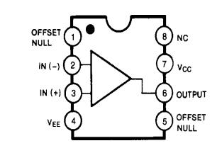
The last image is of a 741 op-amp pin-out diagram, which is the chip I will be using. Double check the pin-out diagram for the op-amp you want to use, especially chips that have multiple op-amps in one package. Positive voltage from your power supply connects to pin 7 and the negative to pin 4. Pin 2 is the inverting input and pin 3 is the non-inverting input. Pin 6 is the output. Pins 1 and 5 are the offset null pins, which are rarely used and so will not be covered in depth here as most op-amps don't even have them, especially in larger dual and quad packages. Pin 8 is not connected.
Step 2: Summer


The summer is used to add two or more voltages together through an input resistor ladder (image 1). The resistors can all be of the same nominal (labeled, not actual) value, or they can be different. If they are different, we get a weighted summer. The equation for Vout is shown in the schematic image. The value of each input is given a percentage, or weight, of the whole. Adding up all of the weights gives you your output, inverted of course because we are using the inverting input. Note that we can still implement gain here, determined by Rf/R.
Build: Connect your (+) and (-) power supplies to pins 7 and 4, respectively. Place all of your input resistors in parallel, connecting one end of all of them together, either in the same row of a breadboard or with jumpers. Leave the other ends of the resistors disconnected from each other, connecting the inputs to one resistor each. Connect the feedback resistor (Rf) across pins 2 and 6. Pin 6 is your output. (Image 2)
From the scope image, we can see that if we input 100mV on both inputs (200mV total), we get 2V out (200mV * 10 gain). (Image 3)
How do we scale our inputs to have more or less weight? Change the values of the input resistors. The math gets a little bit more fun, but not hard at all. -Vout = Rf * (V1/R1 + V2/R2 +...+ Vn/Rn) Images 4 and 5 shows the result of changing the input resistor for V2, first to 500Ω and then to 2kΩ, respectively.
With the input resistors all the same, each input has the same weight, so the total is a simple sum. When the resistance of one input goes down, the gain is now higher, and it therefore has more input into the system, giving more weight to the input relative to the output, which increases linearly. As one input resistance goes up, the gain for that input decreases, while the gain for the other(s) stays the same, so the weight of that one input now goes down. With 500Ω, the gain is 10kΩ/500Ω = 20X. So the 100mV input becomes 2V output, while the other 100mV input outputs 1V. Add them and you get the 3V seen in image 4. If the input is changed to 2kΩ, gain is now 10kΩ/2kΩ = 5X for that input. 100mV becomes 500mV, the other input stays at 10X for 1V output, and we get a total of 1.5V as seen in image 5.
This all comes together very nicely when you want to convert digital signals to analog signals. If you're not familiar with binary numbers and counting, read this. If we assume a 4-bit digital input, with each bit tied to one of four inputs of the summer, then if all bits are 0, we get the lowest value out, 0V. If all bits are high, we get our max voltage as determined by the (+) voltage supply and the gain. As we count up from 0 to 15 in binary on the 4 inputs, we get one of 16 possible analog voltage values coming out of the circuit. For easy math, let's assume a max output of 4V, so for each binary number we count up, we add 4V/16 = 250mV. For this to work properly, we need different values for the input resistors. A quick look at how binary converts to decimal and we see that not all binary digits have the same weight, and they are related by powers of 2. So we adjust our input resistors to match the same relation, with the values of 1kΩ (2^0), 2kΩ (2^1), 4kΩ (2^2) and 8kΩ (2^3) tied to input bits 0-3, respectively. Image 6 shows the output with the scaled resistors with the transition between digital values set at 4ms. The resolution is really rough because of the small number of bits on the input. As mentioned, 4 bits only allow for 16 possible values (2^4). With 8 bits, that grows to 256 values (2^8), with 16 bits we get 65536 (2^16), and 32 bits gives 4.3 billion (2^32). With more values to choose from, we get much higher resolution because each step is smaller and we can manipulate the waveform to provide any shape we want at nearly any frequency just by programming the digital input. This is how the Analog Discovery and EE board generate waveforms.
Image 7 shows what happens to the output when all input resistors are equal and therefore all inputs have equal weight. Definitely not a good waveform.
Step 3: Subtractor


A subtractor is nothing more than a standard differential amplifier (image 1). We saw this before in part 1, step 4, but this time we will use the non-inverting input instead of tying it to GND. When we tied one input to GND, the difference between the two inputs was the actual voltage level at the non-grounded pin. That difference is then multiplied by the gain and we get our output. Now we will measure the difference between two voltages, both relative to ground, and the difference between the two is then amplified. See Image 1. The equation is not difficult, and is simplified to Vout = R3/R1 * (V2 - V1) if we make R1 = R2 and R3 = R4. This gives us a gain of R3/R1. If all 4 resistors are equal, R3/R1 = 1, we have unity gain, and Vout = V2 - V1. Notice that this is exactly the output we get when V2 is GND (0V). 0 - V1 = -V1, which is the output from a unity gain, inverting amp. Nice and simple. For this example I'm using 4 resistors of the same nominal 1kΩ value.
Build: Power supply connections as before, '+' to pin 7, '-' to pin 4. One end of R1 goes to pin 2, with the other end connecting to V1. R3 goes across pins 2 and 6. One end of R2 goes to pin 3, with the other end connecting to V2. R4 connects between pin 3 and GND. Pin 6 is your output. (Image 2)
You can see from images 3 and 4, we get exactly the output we expected. Image 5 shows the same circuit with R3 and R4 replaced with 2.2kΩ resistors, giving a gain of 2.2X to Vout.
Step 4: Differentiator


If you are at all familiar with calculus, you know how to differentiate an equation. If you want/need some more instruction, check out this site from the UK. Basically, we want to know the rate of change, or slope, of a function at a any single given point. If we look at the graph for the function y = x, we see that it is a straight line at a 45 deg angle, rising up from left to right. The fact that it is straight tells us that the slope is constant, with a value of 1, at every point on that line. Thus, the graph of y = 1 is the derivative of y = x.
Electronic signals can be mapped on a graph as functions. That's all oscilloscopes do. By using a differentiator circuit (image 1), we can find the slope of an electronic signal at any given point in time. This is how FM signals are converted to AM signals in your radio so that the carrier frequency modulation can be filtered out and the data (music) can be retrieved. See this Instructable for more on that.
The frequency that we input into the differentiator is actually not super critical. There will be some attenuation at both high and low frequencies, but I've gotten the best response from the circuit when I match the frequency input to the R/C combo according to the equation we've seen before, namely f = 1/(2π * R * C) where f is frequency. However, it is easier to differentiate first and then compensate for any loss with an amplifier later. For this example let's use a 10kΩ resistor and a 1nF ceramic disc capacitor. Have a 47kΩ resistor handy.
Build: Connect power as before. Place the 10kΩ resistor across pins 2 and 6. Connect one side of the capacitor to pin 2 and the other to the input. Pin 3 connects to GND. Pin 6 is your output. (Image 2)
Image 3 shows a sine wave input at 16kHz (red) and a perfect cosine wave output (blue), which is just a sine wave phase shifted by 90 degrees. If you are familiar with calculus, you'll know that the derivative of the sine function is the cosine function. (Yes, I know that the image shows a sine in and inverted cosine out. Remember that we are inverting the sine wave at the input and that the derivative of an inverted sine wave is ... an inverted cosine)
Image 4 shows a triangle wave input. Since the slope is constant, the output is constant, only changing polarity as the slope changes polarity. I switched R1 with the 47kΩ and moved the 10kΩ resistor to between the input and the 1nF capacitor. I then used a 5kHz triangle waveform.
Image 5 shows how the differentiator changes an FM signal to an AM signal. When the input has a higher frequency, the output has a high amplitude, and when the input frequency is low, so is the output amplitude. Also, notice how the output is phase shifted from the input by 90 degrees again. The input here is a 2kHz carrier frequency with a 200Hz modulation frequency, amplitude of 2V, and index of 50%. The circuit is the same as for the triangle wave input.
One drawback to differentiators is that they have a tendency to pass noise from the input through to the output, and are also unstable at high frequencies, so some filters are always nice to have on hand in your circuit after the differentiator to amplify the signal. Just tune the filters to filter the frequency of the noise.
Step 5: Integrator


Integrators are the inverse of differentiators. If you look at the differentiator again, you'll see that it looks really similar to a high-pass filter, with the capacitor out in front of the input. To convert to a low-pass filter, we just place the capacitor across the op-amp. Turns out, the integrator is remarkably similar to a low-pass filter. (Image 1)
Because this is so similar to a low-pass filter, weird things happen at high frequencies, so avoid those. Using the formula for frequency f = 1/(2π * R * C), we can calculate the cutoff frequency of our circuit.
Build: Connect power as before, '+' to pin 7 and '-' to pin 4. Connect the resistor between the input and pin 2. The capacitor goes across pins 2 and 6. Pin 3 is grounded. (Image 2)
In image 3 we see how the square wave input will generate a triangle wave output. This is to be expected as the triangle wave generated a square wave when we passed it through the differentiator. The signal used was a 2V (0-p) square wave at 3.4kHz. Notice that there are some anomalies in the triangle wave. These are due to chip performance characteristics. When I swapped the ua741 for an OP27, image 4 is what resulted with the same input signal.
Image 5 shows the output from a 3.4kHz sine wave input. Notice that it is just a phase shifted sine wave, this time by -90 degrees, just as we would expect the integral of the sine function to look (again, remember that we inverted the sine wave first). Notice that we have the anomalies from the chip as well.
One drawback to integrators is that because there is no feedback between output and input, the 0V point on the output will be arbitrary. Passing the signal through a small 1:1 transformer or high-pass filter, tuned to your frequency needs, will remove the DC bias and center the signal on zero.
Step 6: Square Wave Generator


Waveform generators are circuits that output a constant time varying signal. They can be square, triangle, sinusoidal, ramp up, ramp down, ... etc. The list goes on and frankly, a waveform can have any shape you want it to.
The first example is a square wave generator. This is essentially a comparator connected so that the non-inverting input has a constant reference voltage and the inverting pin has a reference voltage based on the charge/discharge rate of a timing capacitor. As the capacitor voltage goes above the reference voltage, the output swings to the '+' rail. Once the capacitor discharges, the output then swings to the '-' rail. Since charge/discharge cycles are constant, as determined by the RC constant of the circuit, we get a stable square wave output.
The circuit in image 1 is a fully adjustable square wave generator, which is a slightly modified version of one I found in Forrest Mims' book Timer, Op-Amp, & Optoelectronic Circuits & Projects, pg 78. C1, R3, R4, P1, and P2 are the timing elements. Increasing C1 will decrease the output frequency, while decreasing it will have the opposite effect. P1 and P2 are useful for fine tune adjustments, but replacing them to match P1 with R3 and P2 with R4 is perfectly fine. R1 and R2 are used to tune the pulse width. By increasing R1, we widen the pulse width and by decreasing it, the pulse width shrinks. You can also insert a 5-10kΩ potentiometer in between R1 and R2, or even in place of R1 and R2, with the wiper contact connected to the non-inverting pin. To capture the scope image, I swapped P1 and P2 with resistors to match R3 and R4, respectively.
Build: Connect the '+' power supply to pin 7 and tie pin 4 to GND. Connect one side of a 100nF (104) capacitor to pin 7 and tie the other side to GND. Connect the other capacitor between pin 2 and GND and one of the 4.7kΩ resistors between pin 3 and GND. Connect the other 4.7kΩ resistor between pins 3 and 7. Connect the two 100kΩ resistors (or 1 single 200kΩ) in series between pins 2 and 6. Connect the two 22kΩ (or 1 47kΩ) resistors in series between pins 3 and 6. (Image 2)
Image 3 shows the waveform output, running at about 300Hz.
Image 4 shows another square wave generator, this one being simpler to build but not as adjustable. R3 and C1 are the timing elements. As either one increases, the output frequency goes down and vice versa.
Build: Connect the '+' power supply pin 7 and the '-' supply to pin 4. Connect a 100kΩ resistor across pins 2 and 6 and another across pins 3 and 6. Connect the 22kΩ resistor from pin 3 to GND and the 10nF (103) capacitor from pin 2 to GND. (Image 5)
Image 6 shows the output running at about 1.3kHz.
Step 7: Triangle Wave Generator


Remember the integrator we just built? Add an integrator to the output of the square wave generator and you get a triangle wave. Nice and easy. (Image 1)
Build: Connect a second op-amp to power like we connected the second square wave example. Place a 10kΩ resistor between the output from the square wave and pin 2. Connect a 100kΩ resistor and the 100nF (104) capacitor across pins 2 and 6. Tie pin 3 to GND. (Image 2)
Image 3 shows the triangle wave output at the same 1.3kHz as before.
Step 8: Sine Wave Generator


I've always heard that good sine waves are rather difficult to produce. Well, that was a big fat lie. Thanks again to Forrest Mims' book that I mentioned before, I found a ridiculously simple sine wave generator that is remarkably good.
Image 1 shows the schematic. The output frequency is related to the same relation as before, i.e. f = 1/(2π * R * C) where C = C1 = C2 and R = R3 = R4. C3 and C4 together need to be 2X C1, so if you want to modify the output frequency by changing C1/C2, change C3/C4 accordingly. The potentiometer P1 lets you fine tune the feedback to allow the circuit to oscillate. If P1 is larger than R3, it won't oscillate so P1 should be less than R3 to work properly, but if it's too small you will get the output swinging from rail to rail and it will look more square than sinusoidal. This circuit is nearly identical to a notch filter circuit, but the twin-tee filter is tied to the feedback.
Build: This one is kind of a doozy. Connect the power supply, '+' to pin 7 and '-' to pin 4. Connect a 1kΩ resistor (R1) between pin 3 and GND. Connect a 10kΩ resistor (R2) between pins 3 and 6, and two more (R3 & R4) in series between pins 2 and 6. Connect two 10nF (103) capacitors (C3 & C4) in parallel between the junction of R3/R4 and GND. Connect two 10nF (103) capacitors (C1 & C2) in series between pins 2 and 6. Tie the wiper contact of your potentiometer (P1) to one end of P1 and tie that junction to GND. Connect the other end of P1 to the junction of C1/C2. (Image 2)
Built as shown, I got a 1.36kHz output as seen in image 3 with P1 set to about 8.5-9kΩ. Since the frequency out f is inversely proportional to the value of either C1 or R3, increasing either will decrease the frequency out and vice versa. Remember, if you change C1, make C2, C3 and C4 the same value. If you change R3, make R4 match and adjust P1 accordingly until you get oscillation. If you get no frequency out, lower the value of P1. If your output looks like a square and is saturating the op-amp, raise the value of P1
Step 9: That's Probably Good...
Honestly I've barely scratched the surface of what you can do with op-amps. They are so useful in so many applications. There are multiple ways to build many of these circuits as well, so don't get overwhelmed by the options. When you find one that works, stick with it. Don't be afraid to burn up a few components either. You can't get much current out of an op-amp (except the TCA0372. 1A output!), but you can sure try. Parts are cheap but the knowledge you gain from messing up is priceless.
Don't forget to check out Part 1! Please don't hesitate to ask questions in the comments below. You never know when someone else has the same question and that way we can all learn and help each other get bettter. Have fun building!


