Introduction: Customize Your PCB Shape With Easy Steps (Full Beginner Toutorial)


More by the author:


About: Hello Everyone, My name is Abdelrahman but you can call me ICARUS. I love making new and crazy stuff, my passion is tinkering and making. Joined to maker community in 2019, feel free to text me Luv U all
This PCB will be slightly different from other PCBs so Keep Reading carefully
The Component I need
In this tutorial, you will learn various skills that will make up your PCB design skills
This tutorial is meant for beginners and intermediate, we will go through a lot of things so keep attention
Supplies


- ATTINY 44
- 6POS 2-Raw Male Header for ISP
- Right-Angle Male Header 0.1" for FTDI
- 10Kohm Pullup Resistor
- LED
- 1uf Bypass/Decoupling Capacitor
- ISP Programmer
Step 1: PCB Design
For detailed Steps I recommend to Visit these two toutorials Tout1Tout2
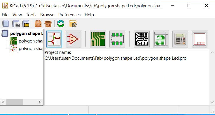
open KiCAd
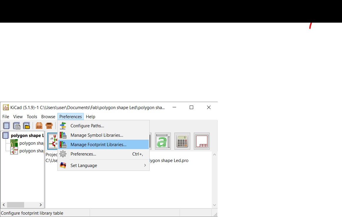
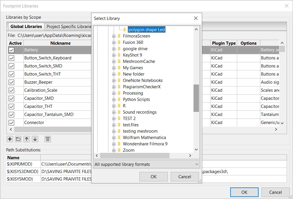
Strat to add Fab modules library
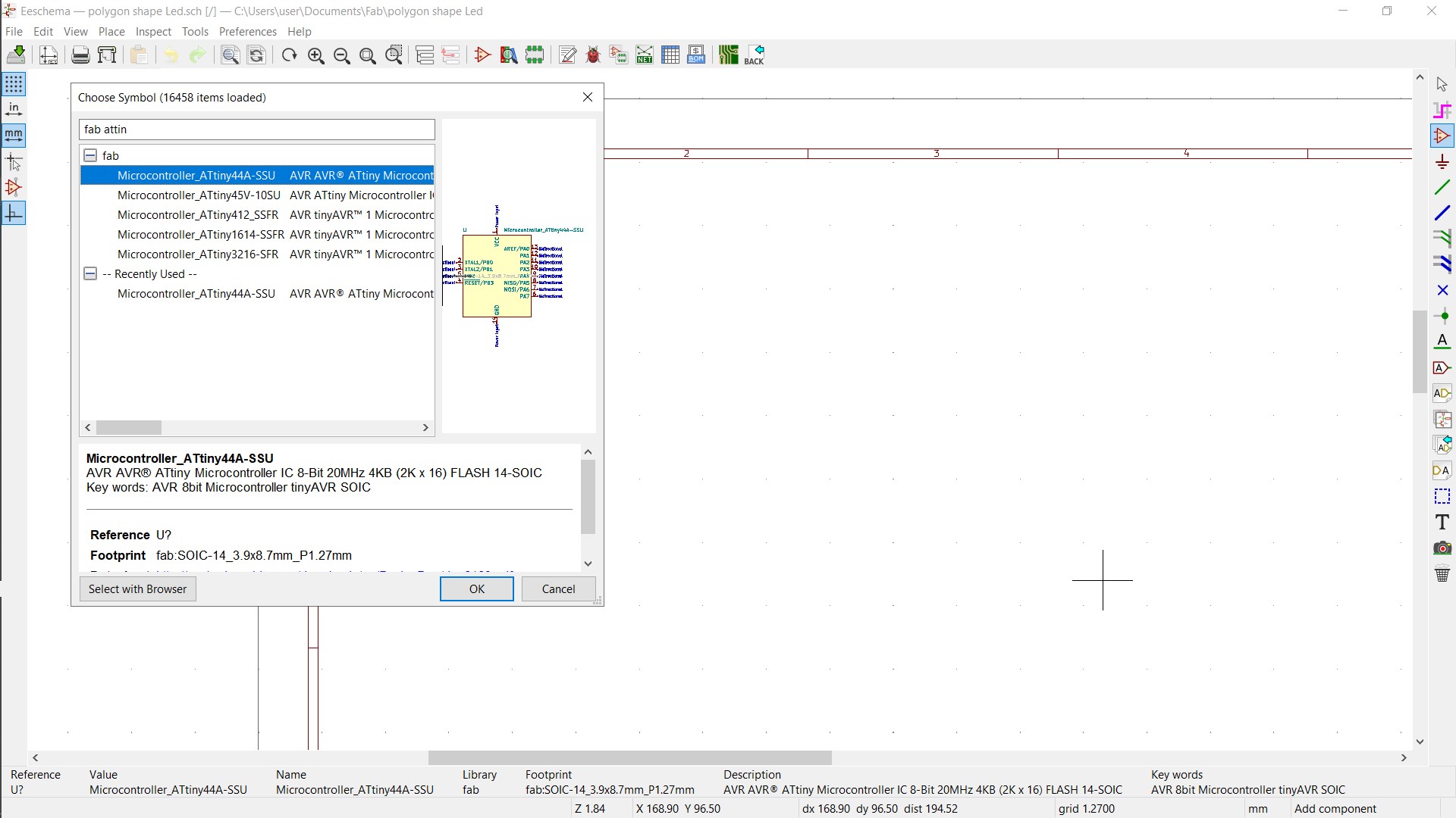
Start to add the Components we need
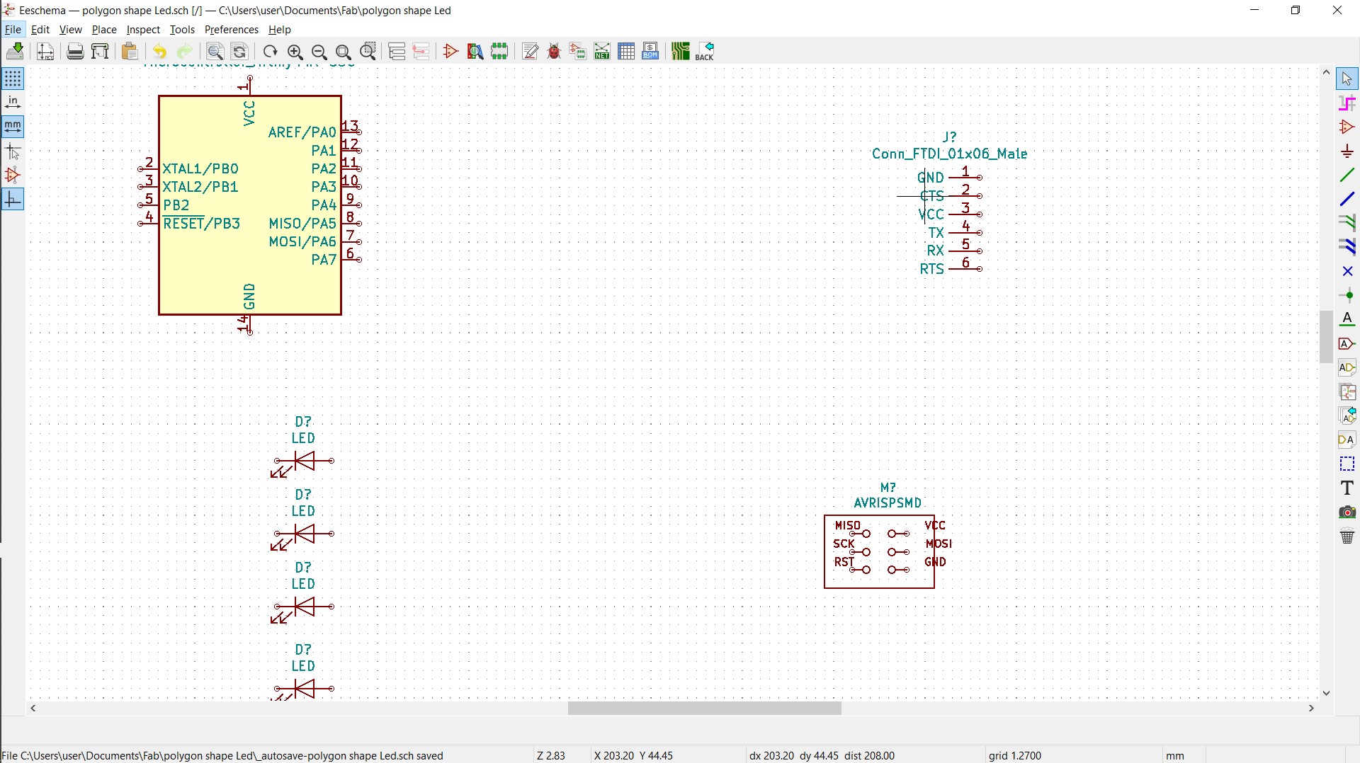
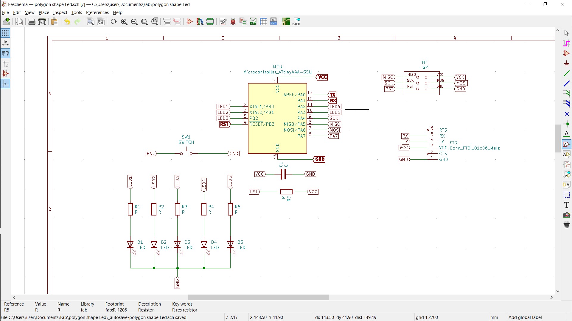
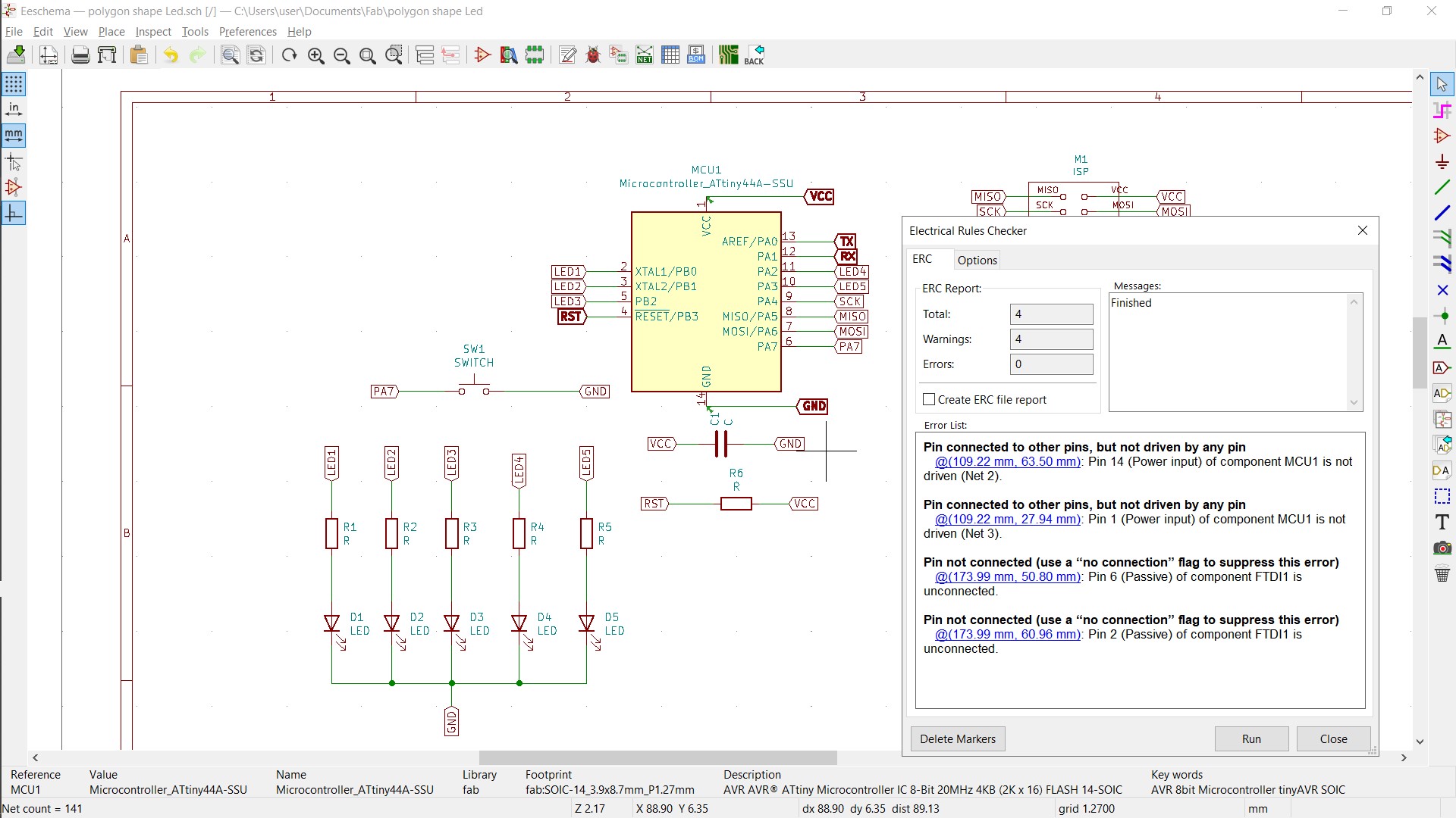
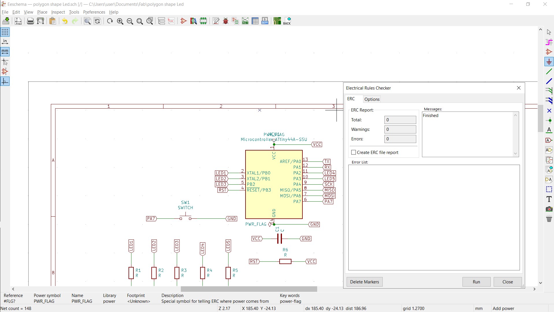
Check the Connections and see if there is an Erorr or not
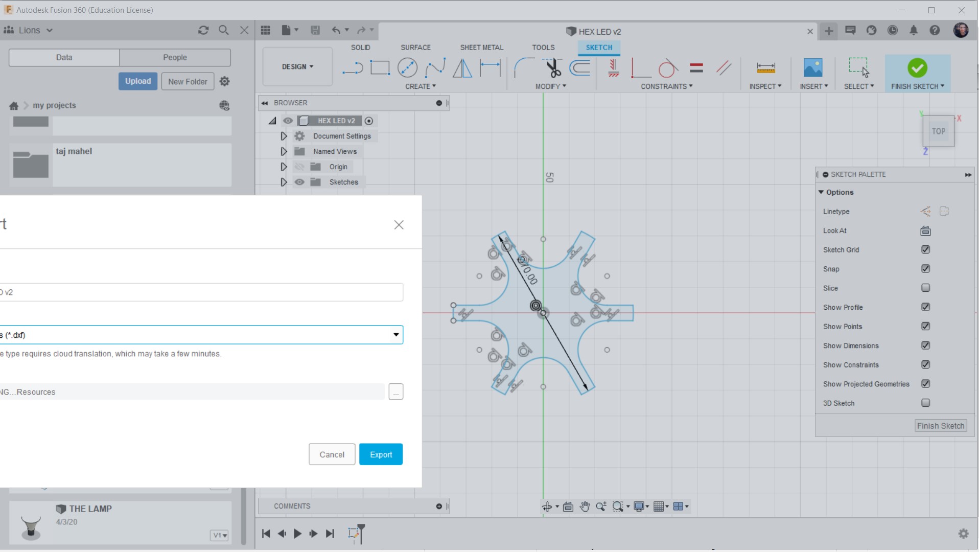
After that Open Fusion 360 Draw the Shape you like And then Save It as a DXF file
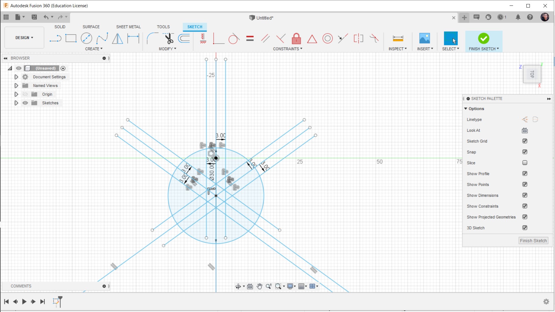
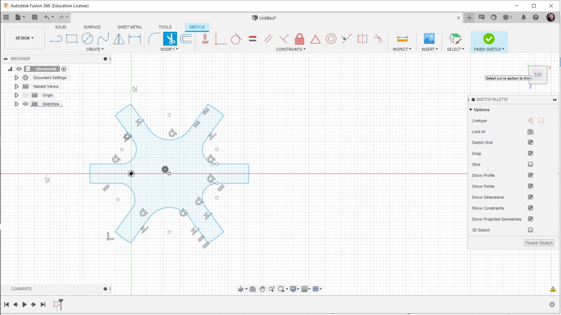
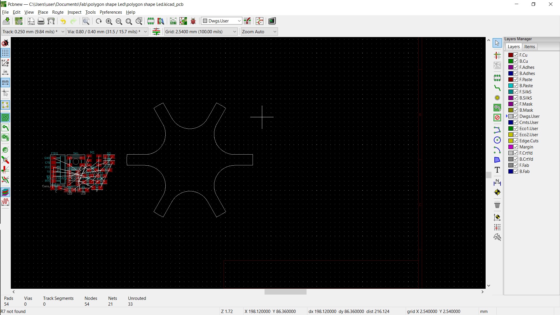
Import the DXF shape to KiCad to make the Connection of the Circuit Inside our shape
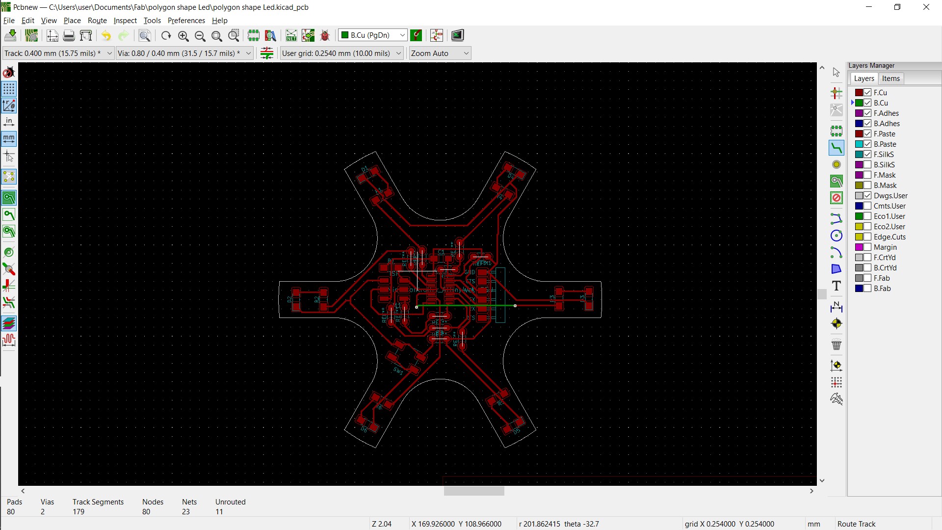
Then Export the Gerper Files
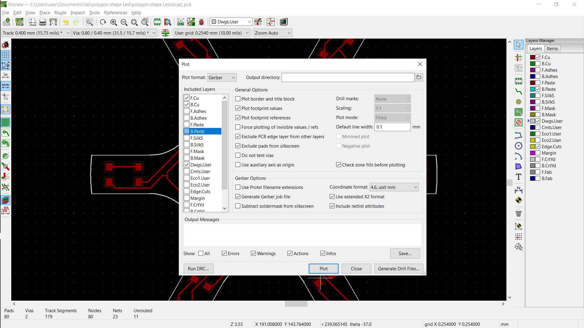
Then after that take the two output images
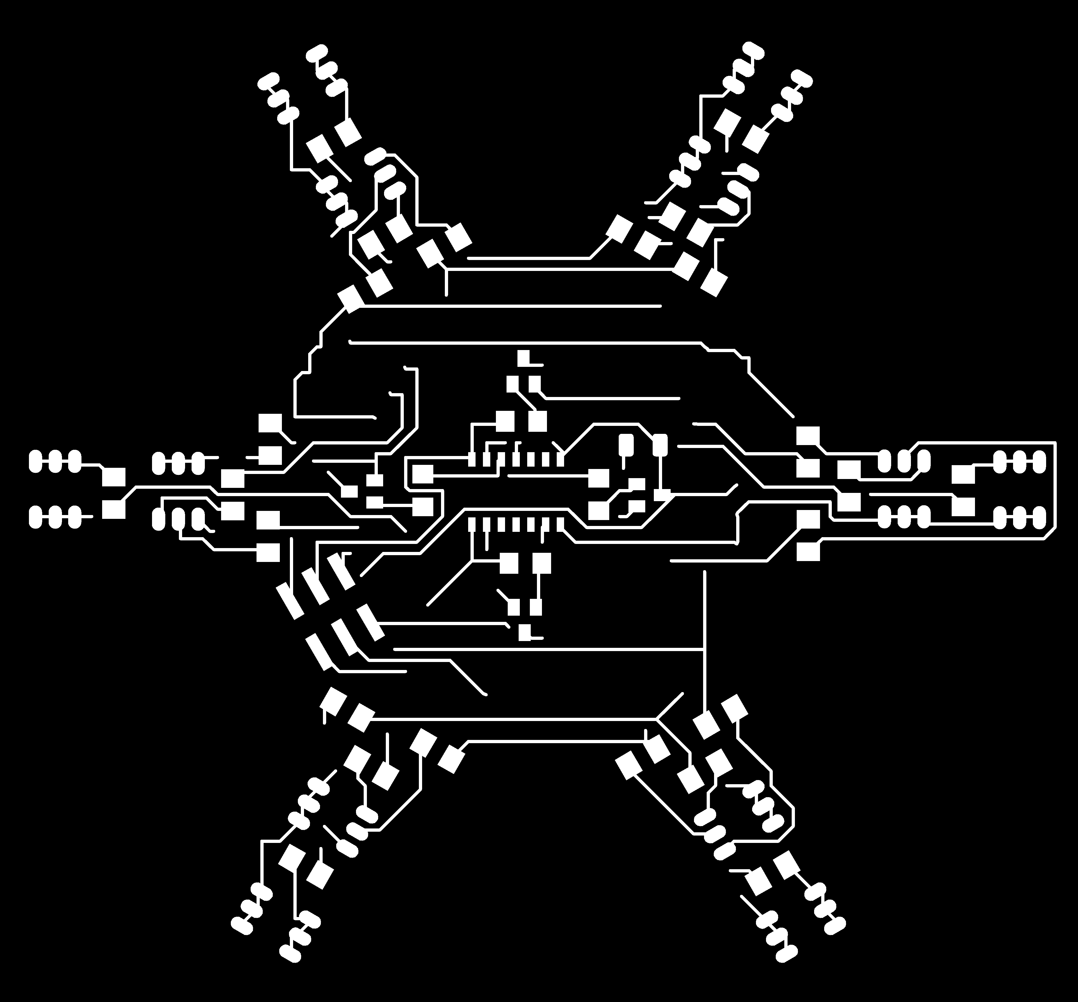
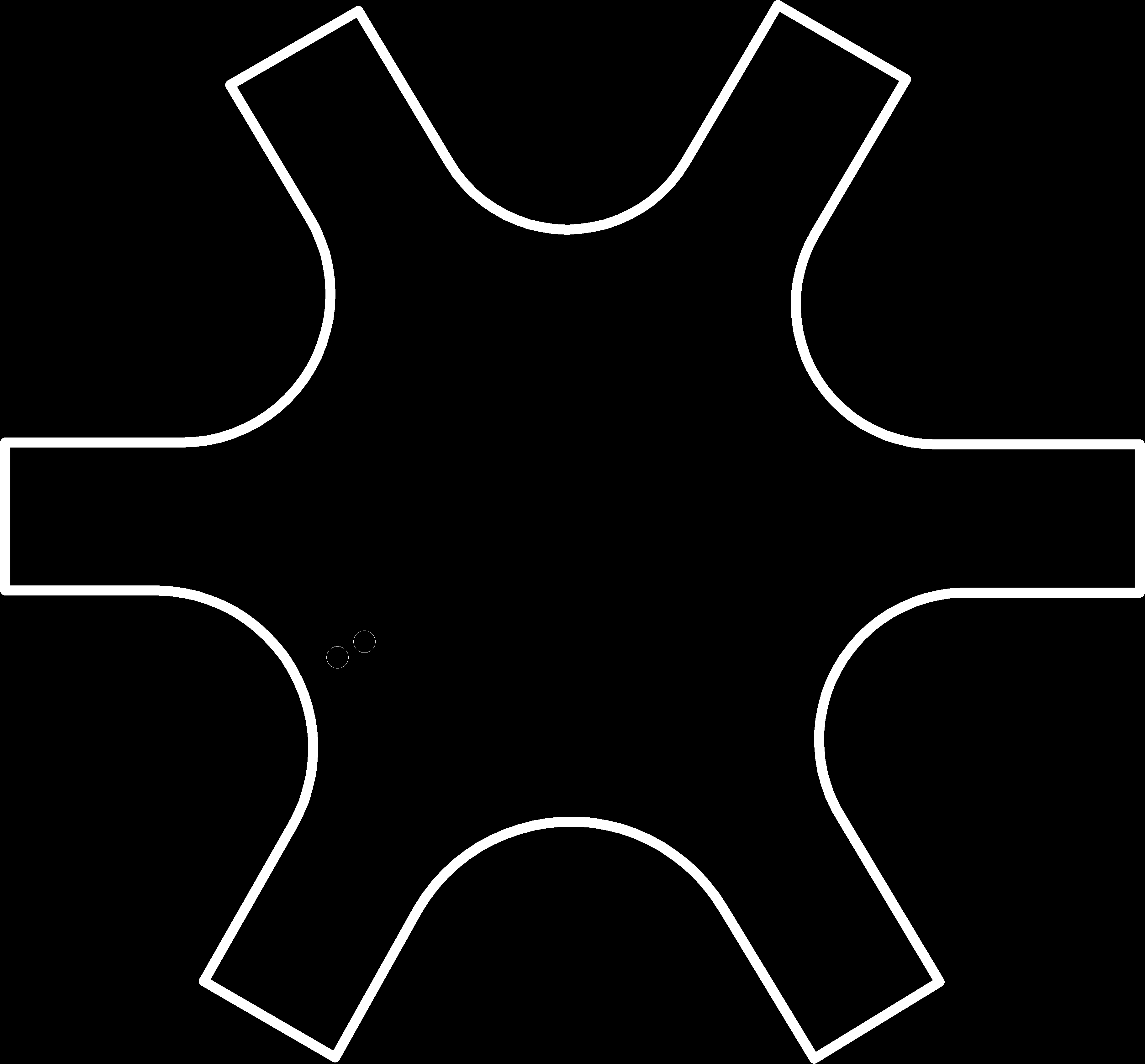
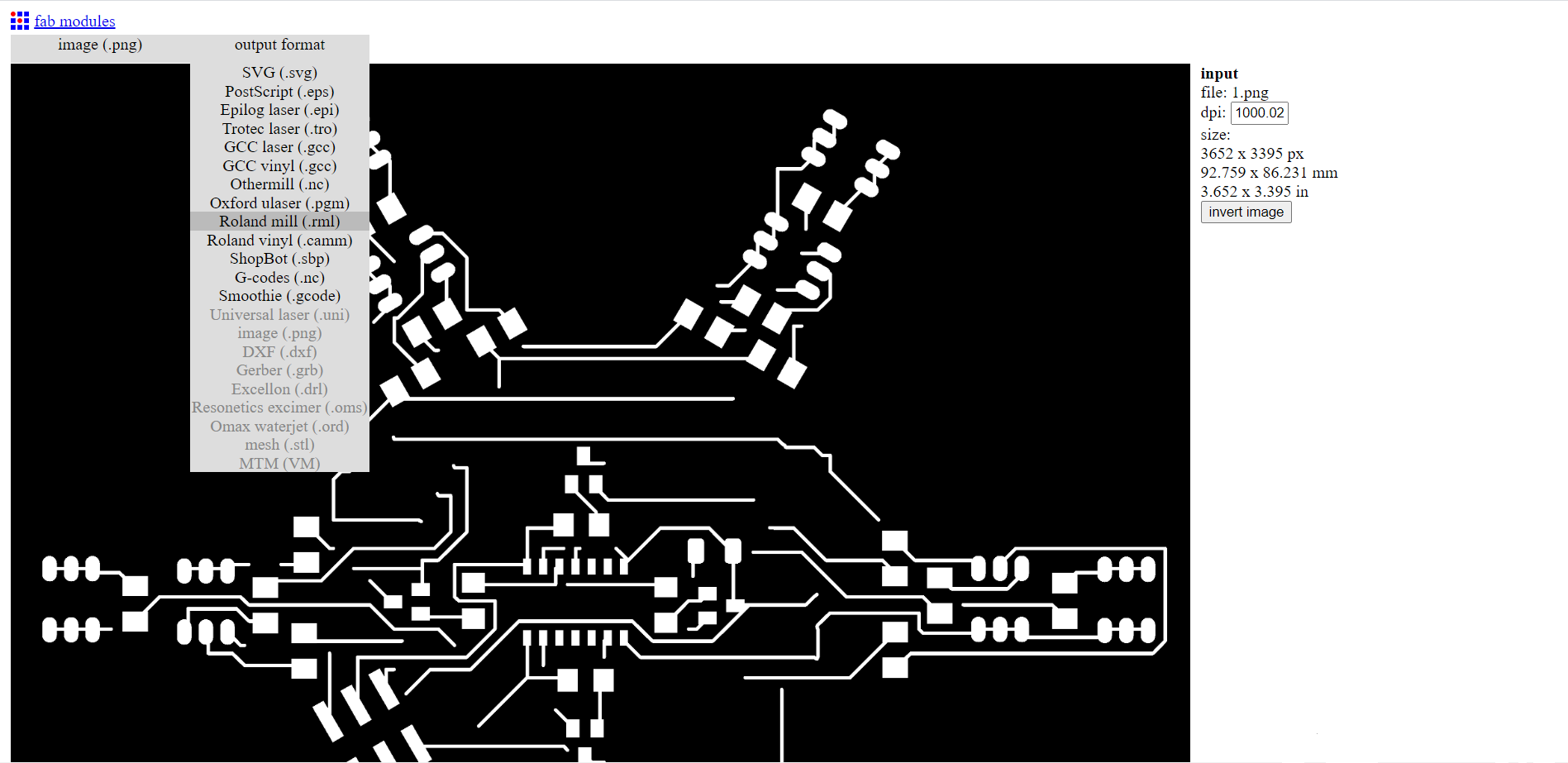
then Open FAB MODULES

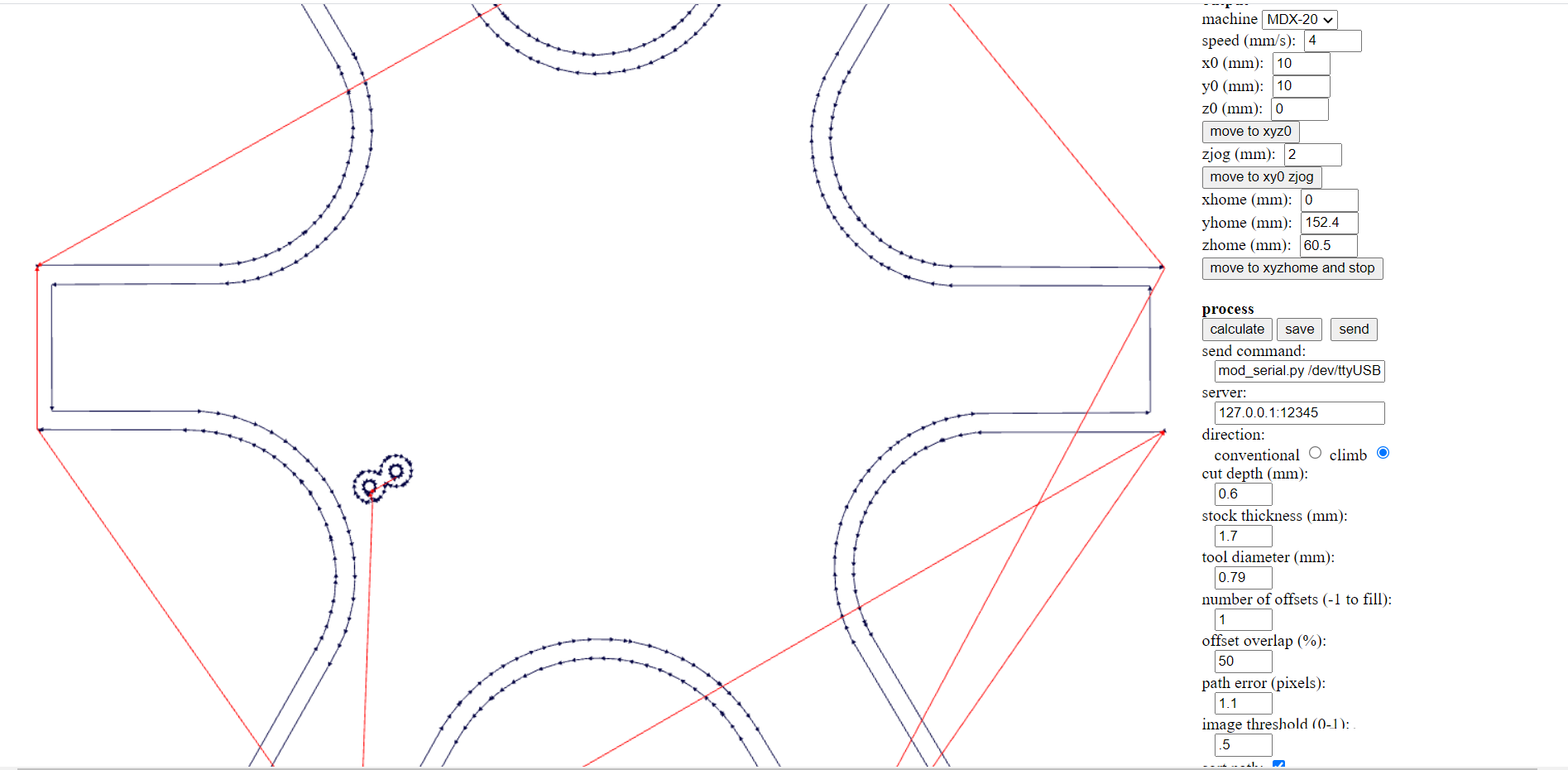
Then Upload the Top layer and choose the output (for me it's role and mill)
Then Choose the PCB Traces (1/64)
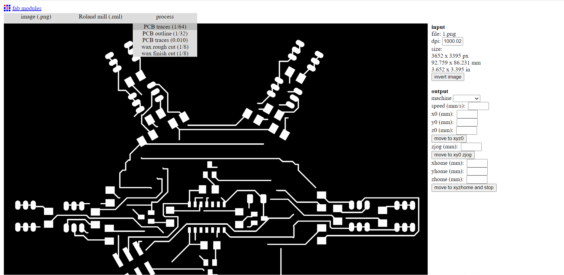
Then make your Preferences and Press Calculate
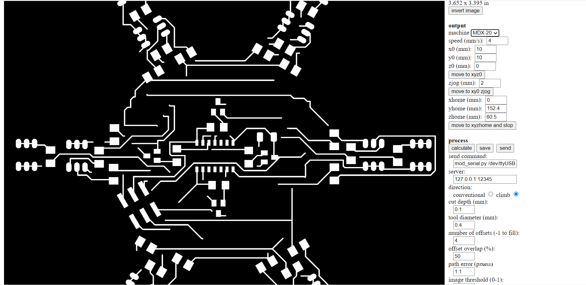
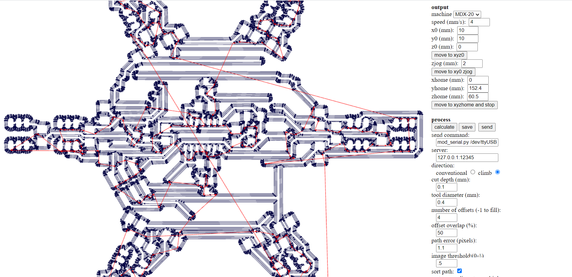
then Send it to the machine
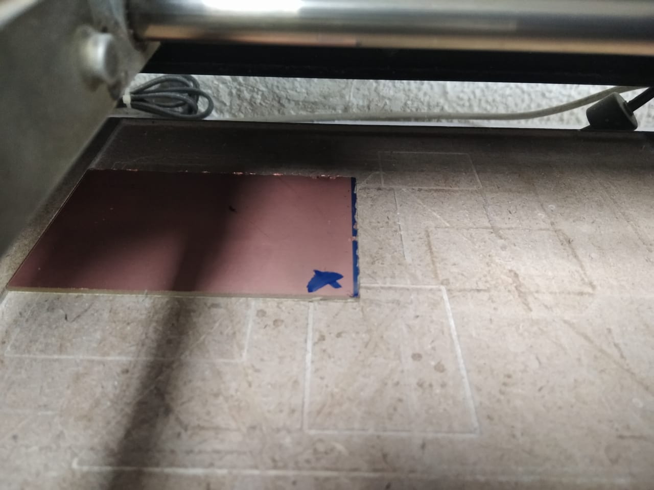
and then make the same thing in the outline
Attachments

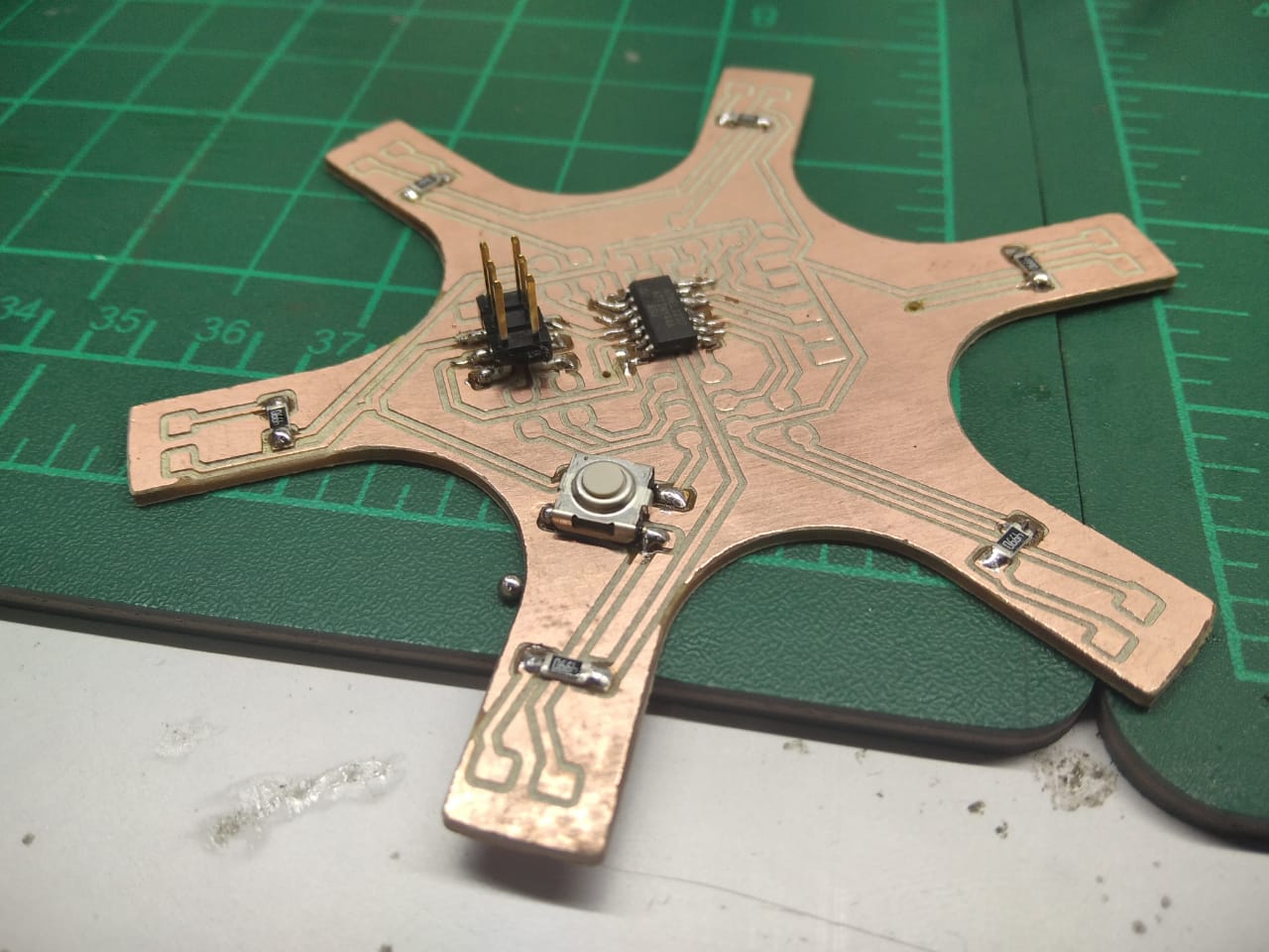
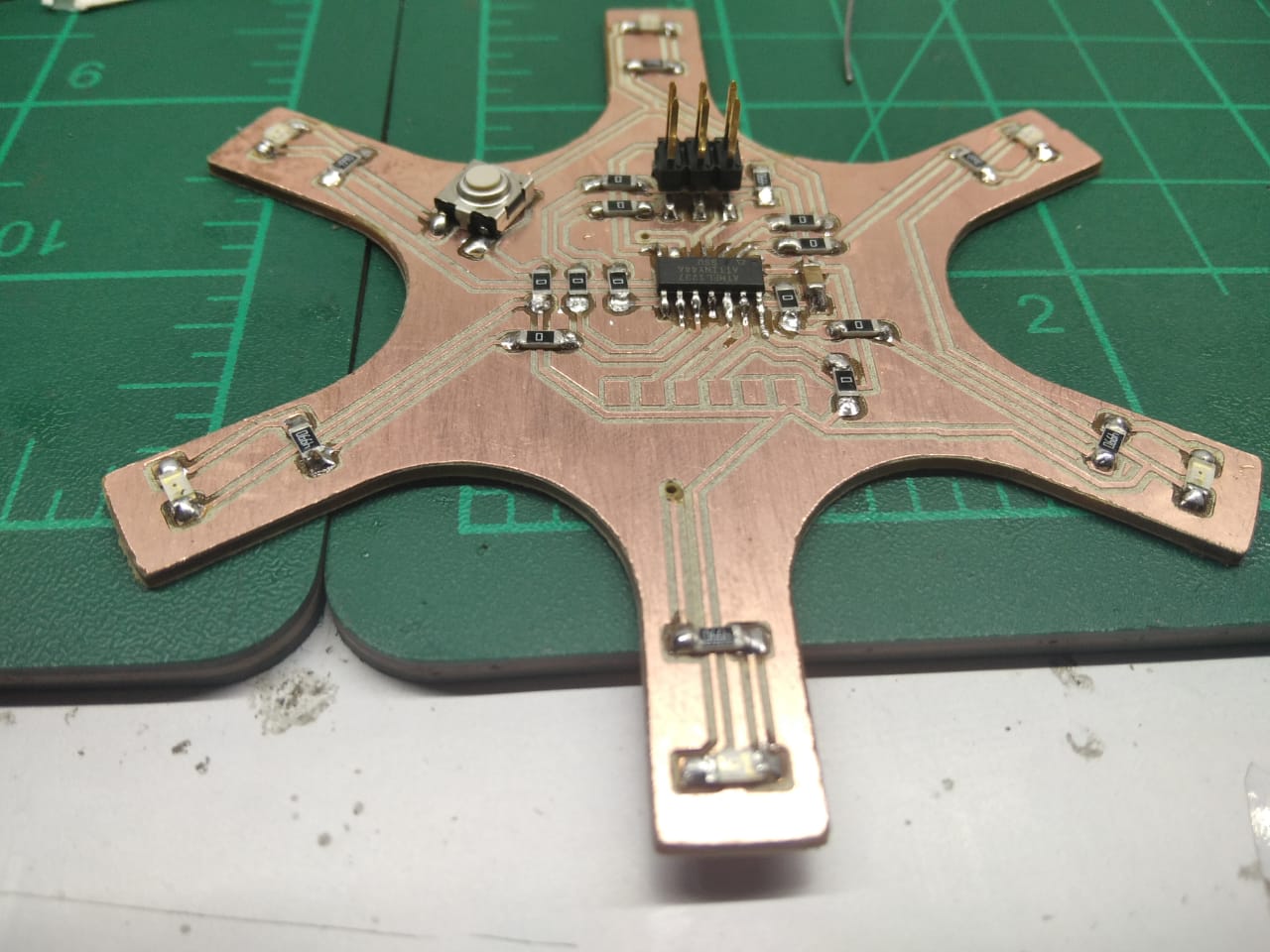
Step 2: Soldering the PCB
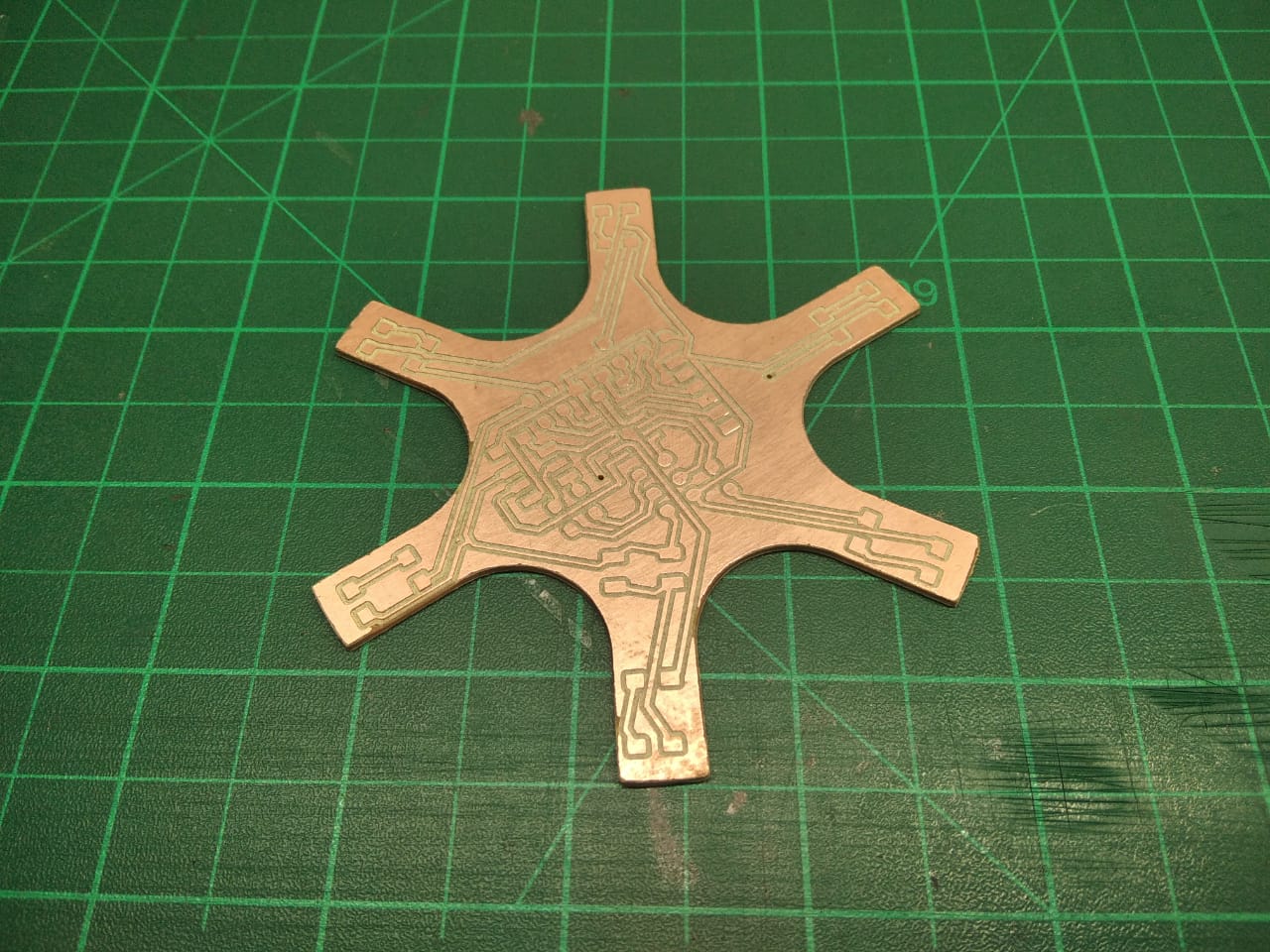
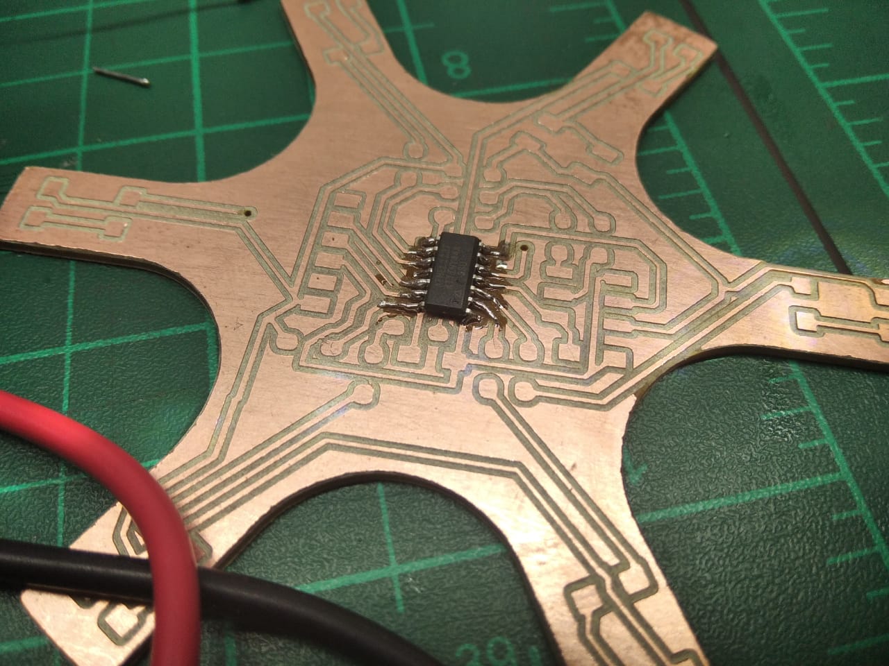
after we Designed out PCB we Fabricate it
and then solder the Component on it
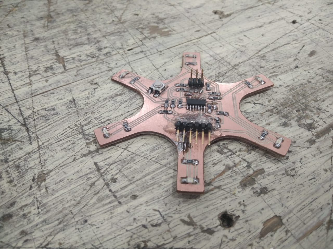
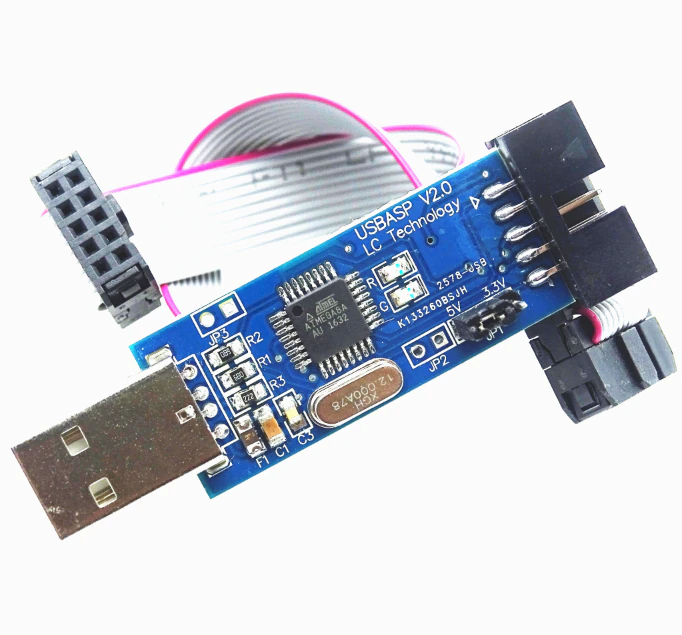
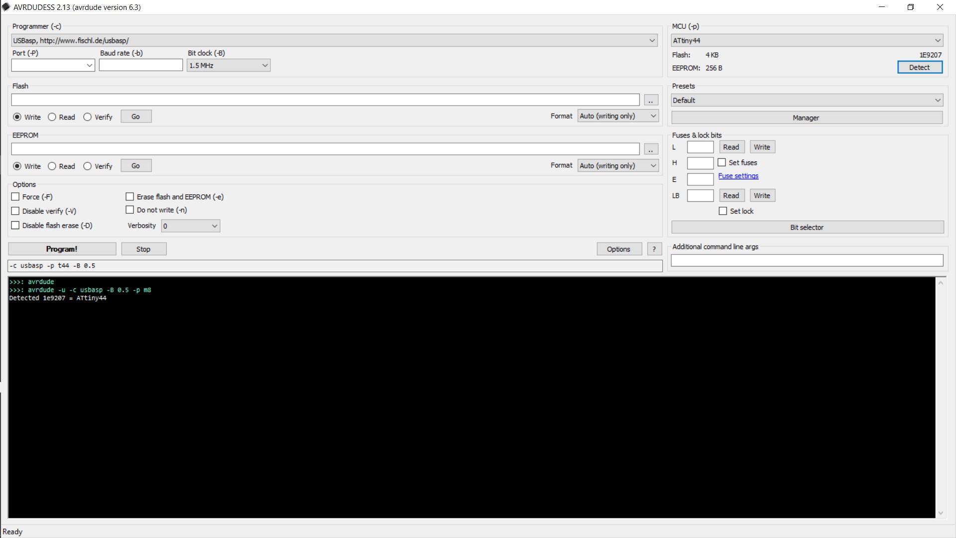
we will use USB ASP to Program the Circuit
We will open AVR DUDES to see if our Circuit working or not (detect the ATTINY44)
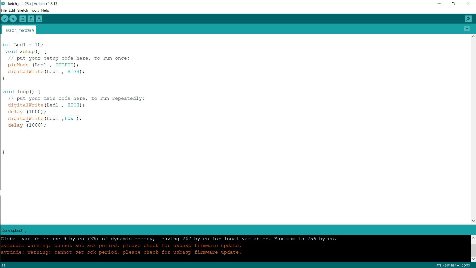
Then we will upload our code to the circuit by Arduino IDE
Attachments

Step 3: Embedded Programming
There will be a full tutorial on Embedded programming on Embedded C
Stay tuned for this Tutorial

![Tim's Mechanical Spider Leg [LU9685-20CU]](https://content.instructables.com/FFB/5R4I/LVKZ6G6R/FFB5R4ILVKZ6G6R.png?auto=webp&crop=1.2%3A1&frame=1&width=306)