Introduction: Weather-based RGB Control: From Idea 2 PCB
Introduction
Well this is a fun project to try and accomplish in quarantine. I thought I would have access to my makerspace’s PCB mill for a couple more weeks, but now I am across the country, trying to figure out if I am going to gain 10 pounds or lose 10 pounds. The next closest thing to a PCB mill near me is the flour mill in the neighboring town.
I decided to take this opportunity to write up a nice instructable on a cool, simple board I made a while ago that can introduce you to the PCB design process: A mounting board for a particle photon to control RGB LEDs. I milled this board using my school's makerspace, the Invention Studio at Georgia Tech.
The reason I wanted to use a photon, rather than just an Arduino is because rather than showing a cool fade between colors, I hooked up the board to wifi and display the weather in a cool way. While I will not focus on the code too much in this tutorial, I will provide it and document it a bit. I thought I would use this board as a nice intro into my PCB design process and workflow.
Essentially, the temperature is portrayed by the color. The temperature varies a lot here in Massachusetts, so I captured from 20 deg F to 100 deg F as a transition from blue to green to red. Green is at 60 deg F.
If you are not familiar with the concept of a PCB and why its useful, think of your remote. If the circuit inside the remote had all these wires and huge components sticking out, it would be difficult to manufacture, difficult to solder, difficult to use, and difficult to look at. A PCB creates a nice, compact, professional wiring between components that is permanent for easy manufacturing repeatability and easiness to integrate into an overall design. A PCB is made of alternating layers of copper and insulation. The copper is cut away in patterns such that it selectively connects parts of a circuit, just like wires do, but in a much more compact manner.
Overview of the design process
As I am sure you must be tired of hearing, design is an iterative process. Luckily, I have done most of the spinning on the proverbial wheel of design iteration, and can advise you on what to do, and, more importantly, what NOT to do.
Before we can even think of designing a PCB, we need to make sure we have a working circuit.
So, an overview of our steps:
- We need a rough idea of how the components go together.
- We need to specify those connections so that we obey electrical principles
- We need to test the circuit on a breadboard with the actual components we are using.
- We need to convert the breadboard model into a PCB design
- We need to mill and test the PCB
Supplies
Hardware:
- 3 x 2N3904 NPN transistors
- 1 x L7805CV 5V voltage regulator
- 3 x 1kOhm resistor
- 1 x 330 Ohm resistor
- 1 x Barrel jack connector
- 1 x Particle Photon
- 2 x Breakaway female headers
- Male & Female JST connectors kit:
- Wire
- Crimping tool or pliers
- E357850 RGB LED strip
- 12 V, 650 mA power supply compatible with the barrel jack connector. You can control about 11 or 12 LEDs reliably with this supply. If you want more LEDs, then you need a 12V supply that can provide more amperage.
Software: we will go through the installation and stuff as it becomes relevant. We will need KiCAD and Particle Photon development things.
Step 1: Circuit Schematic
In order to control the RGB LED strip, the components need to be combined generally in the communication path laid out in the first image. Note how this does not have pins labeled or any passive components. This is just a rough layout used for keeping track of big picture things like power supply and functionality.
We can then make this more specific with a little bit of research. This is my first project with a Particle Photon so google was my best friend. I searched up tutorials for Particle Photon and found that it was well documented and functioned basically like an Arduino, but with a few more setup steps. More on that later. For now, using what I knew about Arduino and circuits, I specified the vague communication diagram above into the schematic attached.
Resistors:
We now have a few resistors in the mix that serve different functions. The 330 Ohm resistor leading to the LED strip is called a current-limiting resistor. We have this here because diodes have very low resistance, which means at 12V supply (what the LED strip takes), the current would be very high and heat up the board, and likely fry it. The 330 Ohm resistor increases the overall resistance of the circuit, and therefore limits the current to prevent frying from happening.
The other set of 1 kOhm resistors are called pull-down resistors. We need these because the pins on the particle photon that they connect to are either ON of OFF but could also be in a third floating state. To make sure that the third floating state does not affect what the circuit reads the voltage as, we tie them to ground to make sure the pin only reads HIGH when ON, and LOW all other times (OFF and floating).
Transistors:
We also have transistors connected to the LED strip. This is to help with PWM control of the LEDs. Transistors act as a digitally controlled switch. This is useful because the LED needs 12V, but most microcontrollers cannot provide 12V. Transistors allow you to use the logic of 3.3V or 5V provided by the microcontroller board to turn on a switch from 12V to the LEDs. This provides isolation between two systems in our circuit and we can use the current provided by the power supply 12V, which is much more than what the microcontroller board can give to the LEDs. This results in better performance for the board/LEDs and cleaner visuals on the LED strip.
Voltage Regulator:
This component serves one simple purpose: the particle photon cannot handle 12V. Its maximum is 5V. Therefore, we need something that guaranteed the voltage going into the photon is 5V. This is what the voltage regulator does. It takes in 12V and outputs 5V with respect to the ground from the barrel jack.
Sidebar: PWM (Skip this if you don’t care)
If you are not familiar with the concept of PWM, I recommend learning in-depth about it because it is very useful, but for the purposes of this tutorial, let me give you an analogy: if you were trying to cook something that needed to be cooked at exactly 100 deg C, but your stove had only 2 settings, OFF and ON (200 deg C). How would you get to the 110 C without burning the food? It would probably look like you putting the pot on the stove for some time and taking it off the stove for some time. Basically, you are cycling the ON and OFF states so that the temperature of the pot reaches a happy medium at 110 C.
Similarly, using transistors, we can give the LED strip either ON (12V) or OFF. To control the color of the light, we need intermediate voltages less than 12. To accomplish this, we are going to turn the color on and off, very rapidly, to reach a happy medium at some voltage below 12V.
This process is more precise than the stove example. The process of pulsing the max voltage to get a lower voltage is called PWM or Pulse Width Modulation. As for the “Width Modulation” part of it, this is how we determine specifically what voltage we get. In the stove example, if you keep the pot on the stove longer, you get closer to 220 C. If you leave it off longer, you get closer to the cold state of the stove. For the LEDs, the longer you leave the 12V pulse ON for, the closer it will be to 12V. This value, called the duty cycle is often represented as a percent. If you say 10% duty cycle, then you are leaving the pulse ON for 10% of the pulse time, and OFF for 90%. Instead of percents, our duty cycle is expressed on a range of 0 to 255. Image 3 has a diagram of what the different parts of a PWM signal.
Step 2: Breadboard and Code
The next step of this project is to make sure the circuit works. This may seem redundant between the design above and the actual PCB, but this process is crucial because this is a low-commitment way of making sure we have wired the circuit properly, connected to all the right pins of the photon, put the transistors in the correct direction, chosen resistor values correctly, etc. This is the step we want to iterate in because its easy to move around wires and components in a breadboard as opposed to a PCB where you solder everything down.
Here is the breadboarded circuit. This picture is not of much use to you, but trust that it mimics the above circuit diagram and that the circuit works.
The proof that the circuit works will be shown in the next few steps when I go through the PCB design process in software.
Sidebar: Code
So, I didn’t intend for code to be the focus of this project, but I will be sharing it, and it would be remiss if I didn’t break it down a bit. The Particle Photon is a really cool tool because it connects to wifi and can therefore access websites for data. While it may seem complicated, all the code does is ask a weather website what the weather is like and changes the color of the LEDs and the flashing speed of the LED based on the temperature and precipitation of the weather. I have attached the code below. For a tutorial on getting you photon set up and getting your first program running on it, use this link: https://docs.particle.io/quickstart/photon/
One thing you will have to set up is something called a webhook in the Particle Photon web IDE. This allows the board to ask for data in a structured manner. Here is a tutorial for setting up a webhook: https://docs.particle.io/tutorials/device-cloud/webhooks/ and I have attached an image showing how I filled out my webhook.
Attachments
Step 3: Intro to KiCAD
The software we will be using is an open source software called KiCAD. This is an open source software where you can insert components and connect them electrically. You can check if all the power and input/outputs are connected properly. You can then place your components how you want, making sure the board will account for everything in your circuit, and connect the components using lines of copper called traces. This layout can then generate cut files to give to either a board manufacturer or for a PCB mill.
There are three steps in this process:
- Lay out the electrical connections in this process
- Associate each electrical component with a physical model
- Lay out the physical components and connect the appropriate pins
From here, we can generate our files to mill the board out and the rest is history.
Here is the link to download KiCAD: kicad.org
Here is a pretty nice video series for learning the workflow in KiCAD: https://www.youtube.com/playlist?list=PL3bNyZYHcRSUhUXUt51W6nKvxx2ORvUQB
Don’t worry too much about watching this full video series unless you are following along with this instructable. Most of learning KiCAD is just getting used to the controls, just like every software.
Play around with it, and you’ll start getting the hang of it.
Alright, so let’s dive into it now…
Step 4: Creating a Project and Downloading the Necessary Library Files
It’s a good idea to keep a folder on you computer for this project as you there will be a lot of files generated with this project, namely a project file (.pro), a schematic file (.sch), a layout file (.kicad_pcb), and the cut files (.gbr, and .drl). This is also a good place to store additional component libraries for this pcb. For this project, we will need the component library for the particle photon as it is not built in.
Download the files from this github and store them in a subfolder to your project folder: https://github.com/coredump-ch/kicad-particle
Now, we open the KiCAD app and see the following screen:
Click File > New > Project
Navigate to the folder you created for the project, name your project and save it here.
Click on the eeschema button and we are now taken to this new program:
Click Preferences > Manage Symbol Libraries > Append Libraries
Navigate to your project folder where you downloaded the .lib file from the github and select it.
Step 5: Designing the Electrical Connections in KiCAD – Eeschema
So, let me make this a bit easier to read by just giving you a few hot keys and some workflow stuff.
- Add a component by pressing ‘A’ – search through the list to find a component.
- Hover over a component and click ‘M.’ Place the component by clicking again
- Select a component by drag highlighting it.
- You can edit properties of a component by hovering over it and clicking ‘E’
Let’s look at a few parts of our circuit as shown in the images above:
- The barrel jack connector and the voltage regulator are our two power modules. The barrel jack accepts the 12V in, and the regulator takes the 12V and brings it down to 5V.
- These connectors are how we access the remaining pins of the photon on the PCB
- This is the jst connector we are attaching the RGB LED strip to.
- The particle photon with all the labeled connections coming out of it.
- This is the three transistors we are using for PWM control. Notice there is a control line and a power line going into the transistor.
- These power flags indicate that the 12V and GND are voltage references for the circuit. The additionally indicate how external power is coming into the circuit. We could have also had one for 5V for the photon, but I chose not to for simplification.
- The final model of the schematic in EEschema
The connections are drawn using the green wire tool on the right-side bar and connecting things according to our breadboarded circuit. Once we have all the components in the diagram and wired up, we need to annotate them. So, click on the annotate button on the top toolstrip. I tend to just automatically annotate the components and change them afterwards. Using the ‘E’ edit menu. Once your components are labeled, you can run the debugger, which is the small red bug button on the top tool strip. Run this to reveal any missed connections or incorrect power connections. When the debugger shows ‘Finished’ with no error list, then you can move to the next step.
Some common errors are that kicad does not like unresolved or floating pins, so you have to use the blue x marker on the right toolbar to indicate an unconnected pin in the software. Other errors are making sure you don’t have power wired directly to ground, you are using the correct pins of your board to connect, and you have the wires touching the endpoints of your components else it might read them as floating. One additional feature that makes PCBs much easier to read is adding tunnels or labels using the label tool. Any pins that are touching tags with the same label are considered connected. You can see I used those these to make the transistors a bit cleaner. The BLUE and BLUE_CTRL tags hanging off the end of the top transistor are labels. They are connected to the blue power line in the strip and the pin on the photon that controls the blue brightness, respectively.
Step 6: Annotating the Schematic
Before I get into this, I should explain a footprint is the physical imprint of the component on the PCB. A footprint includes how the component will be mounted on the board (surface mount, through-hole), the spacing between pins (pitch) and the overall dimensions.
In the top toolbar, select the annotate schematic button and reveal a menu like this:
The difference is that the column of footprints (the right side of the colon) should be empty when you start. For each component, we will find the associated footprint in the left menu and right-hand-side list and double click to assign it. The left side of the screen has the list of footprint libraries and the right-hand side has the specific footprints inside the library.
Use the list in the above image to find the library and footprints to associate with each component.
When you are done, click OK.
Now back in EEschema, click the ‘generate netlist’ button in the top toolstrip. Save the netlist file in your project folder and move on to the next step.
Step 7: Laying Out the Physical PCB
In the main project page of KiCAD, click the PCB New button to open up the layout editor. In the top toolstrip, click the read current netlist button, navigate to your folder and select the netlist file you just generated and read it in. Close this menu.
Using the same controls as EEschema, space out the components like in the image below:
Click Setup > Design Rules
Change the track width to 1mm or 40 mils. This is an overkill width, it does not need to be so thick, but it helps to see the lines. All the thin white lines are connections that need to be made. Select the B.Cu side in the right list (the green layer). Use the wire tool to connect the pins that are indicated by the white thin lines. One thing I did for demonstration is I connected pins using the other side of the board (F.Cu). Notice how the traces show up as red instead of green.
One additional good practice is using what are called “planes” to connect parts of your circuit. A plane is just using all the uncut copper on one side as a connection between pins that share a voltage. I used a ground plane to make it easier to connect all my grounds as it is a voltage level that I have a lot in my circuit. This is useful because it reduces the number of traces you need and adds some safety in the ground connection for components. To do this, I drew a rectangle using the “filled zones” tool in the right-side toolbar.
The last thing we need is an outline that will allow us to cut out the board. We will use the “Edge Cuts” layer in the right-hand list to indicate this. I drew a rectangle around my board with the edge cuts layer selected.
Sidebar: PCB Design
PCB design is not very easy. There are many things that can complicate a PCB. Some of these include multi-sided boards, many components, space restrictions, trace width restrictions, etc. I will try to address a few of these here. Usually PCBs have copper on both sides, which means you can mount components to either side. Something you need to make sure of is that you are placing components and wiring on the correct side. If you have components with pins that go through the board (through-hole), then you have to make sure you are running the traces on the opposite side of the board to the component, else you cannot solder the pin to the trace connection. If you have many components, its likely you will not be able to find a trace routing that connects all the pins without overlapping, so you will have to use something called a “via” which allows you to go through the board and use the other side’s unused space to route your traces. If you are restricted on space, you will have to use vias to maximize the space you have on both sides of the board. The thicker the trace, the more current it can handle. It’s always a good idea to make calculate the trace width needed for the kind of current you are running through your board. The calculator I used: https://www.4pcb.com/trace-width-calculator.html, said my trace width needed to be 0.317 mils, which is way smaller than the PCB mill I was using can handle, so I just decided to go overkill with 40 mils and make it really easy to see. Another last thing I learned is that if you have copper on both sides of your board, it does not matter if you can route your traces on one side of the board, you should cut pads for mounting components both sides of the board to isolate the pins from the surrounding copper on both sides, otherwise the board pins can short to each other. All of these lessons above are unfortunately found out through experience, so even if what I am saying doesn’t make much sense right now, if you have a board in the future that doesn’t work, you have some troubleshooting points.
Step 8: Generating the Cut Files
This step is pretty easy. Click File > plot
Only select F.Cu, B.Cu and Edge Cuts in the left side boxes. In case you haven’t figured it out yet, F.Cu means front side copper, B.Cu means back side copper; these indicate the side you are cutting into. Click Plot. If it prompts you to refill zones, do so. Then click generate drill files. In the new pop up, make sure the file type is Excellion and then click generate drill file. The four files that were created (3 x .gbr and 1 x .drl) are what you would submit to a PCB manufacturer or to a PCB mill to cut out.
Sidebar: Adding labels
Just like commenting your code is a good idea, labeling your components on your pcb is a good idea too. Do so by adding text in the F.SilkS layer. While this cannot be read by a personal PCB mill, if you give this file to the manufacturers, they can include it on you PCB. When you see a green PCB with text on it, that is using the silkscreen layer to insulate, beautify and label the PCB.
Step 9: Milling and Building the PCB
This step is usually out of your hands. You can get this PCB made using a service like JLPCB or OSHPark. You submit these four files and a week or so later, you will get these bare PCBs in the mail.
I happened to have access to a PCB mill, so I made this one myself. If you mill it yourself, one thing you will want to do is have a multimeter close by to make sure the traces cut out properly. By running some continuity checks. If you have bridged or shorted connections, that would be really bad for the board, your components and your safety. While milling an entirely new board might be a headache, it’s better to get it right than risk it. I have attached two simulated images of what the PCB looks like when its done. And this is rather accurate, save for the green color and labels.
Once you have the bare PCB, you can solder the components on. Place the components in their respective locations and follow this simple sparkfun guide to soldering pcb mounted parts. The PCB makes it easy to solder the components, but you still want to make sure you are not adding too little solder that it makes a weak connection, or too much that it bridges the insulation and shorts something. I also used the female headers on the PCB rather than soldering the photon directly to the board so that it is easily removable.
Step 10: PCB in Action
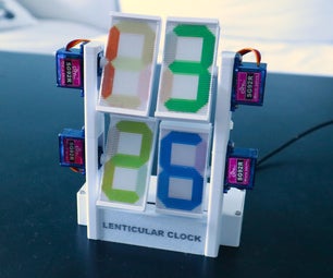
Here is the final PCB in action. I have linked all my design files in this instructable. I used the jst connector with crimped connectors to make a removable connection from the LEDs to the board. In this video, I test out the color change using synthetic, hard coded weather IDs and temperatures and upload the code to see the light flashing. I was testing if the light cycled through blue, and red and changed the flash speed based on severity of precipitation. In the first video we see the color change based on two input temperatures. In the second video we see the lights flicker as a result of precipitation in the weatherID. These LEDs are mounted on the back of a clock I designed. The clock tells time and also now shows the weather.
Thanks for chilling with me through this instructable! Here are the KiCAD files associated with this project: https://github.com/siddharthSal99/RGB-LED-Weather-Control-Photon. Hopefully it was fun and informative. Stay safe until next time!

Participated in the
PCB Design Challenge


